
1Lauren Consulting Ltd., Bartók B. u. 92-94/A, H-1113 Budapest, HUNGARY
2Department of Organic Chemistry, NMR Laboratory, University of Debrecen, Egyetem tér 1, H-4010 Debrecen, HUNGARY
In case of a two spin system we have first experimentally studied and measured connectedness and separation defined by the EQP (Extended Quantum Particle) model. We have prepared an EPR state of the labelled chloroform 1H and 13C nuclear spins and measured the related density matrix by NMR quantum state tomography. We discuss some consequences of these experimental findings for quantum computing and molecular recognition processes.
[1] I. L. Chuang et al., Proc. R. Soc. Lond. A 1998 454, 447-467
[2] Z. Árvay, presentation on EUCOST conference and Scientific Report COST Action MP0802, 2009
CNR-Institute of Nanoscience, via campi 213/A – 41100 Modena, Italy
M-DNA is a type of metalated DNA obtained from the complexation of base pairs with metal ions. Experiments carried-out on Zn-DNA suggested a metallic behavior, with an insulator-metal transition from the natural DNA. We inspect if and how the possible electronic coupling between the metal and the nucleic acid bases may be responsible for such a transition [1]. The effect of other metals such as Cu and Ag [1] is also taken into account to inspect which metal elements are most suitable to perturb the electronic structure of DNA in a desired way. An alternative way to go beyond the limits of native-DNA for nanotechnology impact is to design and syntesize more conductive structures by chemical modifications of the nucleobases. One particular approach relies on the expansion of each natural base with a benzene ring that is covalently bonded to the base and co-planar with it: xDNA [2]. Recent findings reported enhanced stacking interactions in xDNA duplexes and suggested they might be suitable molecular-wires. Here we investigate possible ways of tailoring the DNA electronic structure by combining the metal-doping and aromatic insertion, namely M-DNA and M-xDNA (Figure 1). DFT calculations of the electronic structure are performed, with several localized basis sets, different exchange-correlation functionals, with and without implicit solvent. We analyze the stability properties of salient selected structures. We show [1,3,4] efficient hybridization between the metal and the natural (or expanded) bases, with the possibility of gap modulations (shrinking or enlargement) by using different metal species, which may be the key to electrical non-linearities toward DNA-based nano-circuits. This line of research can also complement the experimental investigation of M-DNA via electron tunneling spectroscopy [4].
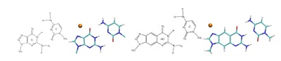
Fig 1. DNA, M-DNA, xDNA, M-xDNA (from left to right) schemes and optimized structures
[1] G. Brancolini and R. Di Felice, “Electronic properties of metal-modified DNA base pairs”. J. Phys. Chem. B 112, 14281 (2008).
[2] J. Gao, H. Liu, E. T. Kool, “Assembly of the Complete Eight-Base Artificial Genetic Helix, xDNA, and Its Interaction with the
Natural Genetic System”
, Angew. Chem. Int. Ed. 44, 3118 (2005).
[3] G. Brancolini and R. Di Felice, “Combined effects of metal complexation and size expansion in the electronic structure of DNA
base pairs”, (manuscript in preparation).
[4] (a) G. Brancolini, E. Shapir, A. B. Kotlyar, R. Di Felice, D. Porath, “Evidence of gap modulation in DNA by complexation with metal
ions”, (manuscript in preparation). (b) E. Shapir, A. Calzolari, C. Cavazzoni, D. Ryndyk, G. Cuniberti, A. B. Kotlyar R. Di Felice, and
D. Porath, “Electronic structure of single DNA molecules resolved by scanning tunneling spectroscopy”, Nature Materials 7, 68
(2008). 9
1Departamento de Química, Faculdade de Ciências e Tecnologia, Universidade de Coimbra, Portugal,
2Institute for Research in Biomedicine, IQAC-CSIC, CIBER-BBN Networking Centre on Bioengineering, Biomaterials and Nanomedicine, Barcelona, Spain.
DNA adsorption on electrode surfaces is of fundamental interest for the development of DNA-based biosensors. The adsorption and the redox behaviour of thrombine binding aptamer (TBA) and extended TBA (eTBA) were studied using atomic force microscopy and voltammetry at highly oriented pyrolytic graphite and glassy carbon. The different adsorption patterns and degree of surface coverage were correlated with the sequence base composition, presence/absence of K+ and voltammetric behaviour of TBA and eTBA. In the presence of K+ only a few single-stranded sequences present adsorption, while the majority of the molecules form stable and rigid quadruplexes with no adsorption. Both TBA and eTBA are oxidized and the only anodic peak corresponds to guanine oxidation. Upon addition of K+ ions TBA and eTBA fold into quadruplexes, observed by the decreasing of guanine oxidation peak and occurrence of a new peak at higher potential values due to the oxidation of G-quartets. The higher oxidation potential of G-quartets is due to the difficulty for electrons transfer from the inside of the quadruplex to the electrode surface than from the more flexible single-strands.
University of California, Santa Barbara
Atomic force microscopy (AFM) is conceptually simple, yet very powerful microscopy technique, which is essential for studying programmable self-assembly process of DNA and RNA nanostructures. Although originally developed for based on tunneling effects in near contact of semiconductors it is now mostly used to image non-conducting samples particularly organic as well as inorganic specimens at the atomic and molecular scale by measuring the forces between the tip and the sample. Since AFM can produce high- resolution topographical images at the nanometer level without altering the sample with stains, it bypasses the problem faced by other techniques such as the scanning electron microscopy. Here we will discuss using atomic force microscopy for various biologically relevant applications. Particularly it becomes an essential analysis in rationally design of artificial DNA and RNA 2D scaffolds. Additionally we will present imaging of protein crystals, surfactants as well as living organisms where AFM serves as a platform for biomaterials surface analysis. Very important is to identify challenges and advantages of AFM over other compatible methods and how important is understanding of your molecule to molecule and sample to surface interactions.
1Institute of Physical Chemistry, Friedrich-Schiller-University Jena, Helmholtzweg 4, 07743 Jena, Germany
2IPHT - Institute of Photonic Technology, Albert-Einstein-Straße 9, 07745 Jena, Germany
Raman spectroscopy is an important analytical tool as it allows the highly specific detection and
identification of molecules and even biological particles. However, the Raman effect is intrinsic weak, but
Raman signals get efficiently enhanced by the interaction of molecules with a nanostructured metallic
surface (for example metal nanoparticles, roughened metallic electrodes or metal island films) yielding in
the so-called surface enhanced Raman spectroscopy (SERS). [1] Through the combination of the SERS effect
with scanning probe microscopy (SPM) the so-called tip enhanced Raman spectroscopy (TERS) is created.
This technique combines the spatial resolution of various SPM techniques (such as atomic force microscopy
– AFM or scanning tunneling microscopy – STM) with the highly specific spectroscopic information of
Raman spectroscopy at a nanometer scale. [2]
Within this contribution the application of TERS for the scanning and identification of biological (sub-µm)
compartments is presented. First investigations within our group of this technique towards the
investigation of complex biomolecules were performed on single bacterial cells, illustrating the great
capability for nanobiological applications. However, spectral fluctuations in band position and intensity are
interpreted as indication of fluctuations of molecules within the outer cell membrane. [3] A further
milestone towards powerful nanobioanalytics are our TERS investigations of single virus particles, being a
promising tool for single virus identification in future work. [4] Moreover the TERS technique was applied
for investigations of supported lipid structures and human cells. [5]
[1] Hering, K.; Cialla, D.; Ackermann, K.; Doerfer, T.; Moeller, R.; Schneidewind, H.; Mattheis, R.; Fritzsche, W.; Roesch, P.; Popp, J.
Analytical and Bioanalytical Chemistry 2008, 390, 113-124
[2] Deckert-Gaudig, T.; Bailo, E.; Deckert, V. Journal of Biophotonics 2008, 1, 377-389.
[3] Neugebauer, U.; Roesch, P.; Schmitt, M.; Popp, J.; Julien, C.; Rasmussen, A.; Budich, C.; Deckert, V. ChemPhysChem 2006, 7, 1428-
1430.
[4] Cialla, D.; Deckert-Gaudig, T.; Budich, C.; Laue, M.; Moeller, R.; Naumann, D.; Deckert, V.; Popp, J. Journal of Raman Spectroscopy
2009, 40, 240-243
[5] Böhme, R.; Richter, M.; Cialla, D.; Rösch, P.; Deckert, V.; Popp, J. Journal of Raman Spectroscopy 2009, 40, 1452-1457.
Dr. Krassen Dimitrov
e-mail: k.dimitrov@uq.edu.au
Direct digital counting (DDC) of biomolecules offers sizable advantages over existing analog technologies in
terms of accuracy, sensitivity, robustness and cost-effectiveness. Nanobarcodes are naometer-sized
structures with high combinatorial diversity that can be used for DDC to compile of virtual biomolecule
inventories from biological samples. Such direct barcoding approach opens unique new opportunities for
biomedical applications.
Fluorescent nanobarcodes rely on conventional microscopic technologies for their optical detection and
identification. These fluorescent structures, or nanostrings, are already finding commercial applications and
outperforming existing bioanalytical techniques.
Electronic nanosensors with dimensions comparative to those of individual biomolecules are becoming
feasible at the latest nodes of CMOS fabrication. Nanobarcodes for electronic detection with such electronic
nanosensors would further advance miniaturization, cost-efficiency and thoroughput, however, they require
fundamentally different technological approaches. One specific technological difference is the requirement to
dynamically control the passage of the nanobarcodes through an electronic nanodetector. To address this
challenge, model dumbbell structures were developed and characterized and their precise dynamic control
was achieved and characterized via magnetophoresis.
Biography
Dr Dimitrov is a Group Leader within the University of Queensland’s, Australian Institute for Bioengineering
and Nanotechnology (AIBN) a position he has held since 2006. Prior to this he was the Founder and CTO of
NanoString Technologies in Seattle (2003-2006), a company he founded to commercialize his invention of
fluorescent nanobarcodes for single molecules.
Prior to NanoString, Dr. Dimitrov was the Director of the DNA Microarray Laboratory at the Institute for
Systems Biology in Seattle (2000-2003), and played a significant role in the formation and early growth of
the Institute.
During his research career Dr. Dimitrov has made many significant research discoveries. Most importantly he
invented and pioneered the barcodes for single-molecule detection, which are currently on the market and
finding diverse applications in biomedical research, diagnostics, biosurveillance. Dr. Dimitrov's current focus
is on a new generation of nanobarcodes that combine magnetophoresis and electronic detection and hold
the promise to be significantly smaller, less costly, and more user-friendly than the NanoString product.
Dr. Dimitrov holds a Ph.D. in Biochemistry from Baylor College of Medicine
University of California San Diego, Department of Nanoengineering and Department of Bioengineering, La Jolla, CA 92093-0448, mheller@ucsd.edu
An electronic microarray has been used to carry out directed self-assembly of higher order 3D structures
from biotin/streptavidin, DNA and enzyme derivatized nanoparticles. Structures with up to fifty layers of
alternating biotin and streptavidin, DNA and enzyme nanoparticles were fabricated using a 400 site CMOS
microarray system. In this process, reconfigurable electric fields produced by the microarray were used to
rapidly transport, concentrate and accelerate the binding of 40 and/or 200nm nanometer bio-derivatized
nanoparticles to selected sites on the microarray. The nanoparticle layering process takes less than one
minute per layer. The nanoparticle addressing/binding process was monitored by changes in fluorescence
intensity as each nanoparticle layer was deposited. The final multilayered 3-D structures are about two
microns in thickness and 50 microns in diameter. More recently we have successfully fabricated enzyme-
nanoparticle layers with streptavidin-alkaline phosphatase, glucose oxidase-avidin, and streptavidin-HRP. Up
to 47 layers were addressed with 200nm nanoparticles and enzyme activity was retained in the assembled
structure. Most recently, we have used AC dielectrophoretic techniques on a 100 site microarray device to
carry out the manipulation and positioning of DNA derivatized nanopartilces. This work represents a unique
example of combining “top-down” and “bottom-up” technologies into a novel nanofabrication process. Such
processes will be useful for the hierarchal assembly of 3D nano, micro, and macrostructures for a variety of
electronic/photonic, nanomaterials, energy and biosensor applications.
Michael J. Heller received his Ph.D. in Biochemistry from Colorado State University in 1973. He was an NIH
Postdoctoral Fellow at Northwestern University from 1973 to 1976. Dr. Heller was supervisor of the DNA
Technology Group at Amoco Corporation from 1976 to 1984, and then the Director of Molecular Biology at
Molecular Biosystems, Inc., from 1984 to 1987. He then went on to Integrated DNA Technologies, where
he served as President and Chief Operating Officer from 1987 to 1989. He was the Chief Technical Officer at
Nanogen, Inc., located in San Diego, California form 1993 to 2001. Dr. Heller is now a professor in the
departments of Bioengineering and Nanongineering at the University California San Diego. He also serves as
a consultant to Nanogen. Dr. Heller has extensive industrial experience in biotechnology; with particular
expertise in the areas of DNA probe diagnostics, DNA synthesis, and fluorescent-based detection
technologies. He has been the founder of several high technology companies. Nanogen Inc., the most
recently formed is directed at the development of novel microelectronic DNA array technology. He has
numerous patents and publications related to his work in biotechnology, on DNA arrays and in the medical
diagnostics areas. Dr. Heller has also served on several review panels for the National Nanotechnology
Initiative.
The mechanical properties and the deformation behaviour of biological cells are mainly determined by the
cytoskeleton. These properties are closely linked to many biophysical and physiological events in the cells,
and may, thus, be exploited as potent biomarkers.
We propose an advantageous approach to characterize cellular mechanical properties: through the
application of dielectrophoretic forces, different types of cells are stretched between microelectrodes.
We first apply our newly developed dielectrophoretic stretcher to compare cell lines that have been derived
from malignant and non-malignant tissues. Small numbers of human cells of cancerous origin and from
related non-cancerous tissue were sufficient to obtain data that allowed for unambiguously distinguishing
these cells. By applying our technique to malignant and non-malignant mouse fibroblasts, we observed a
deformation response to the electric field that confirmed the results obtained from the human cells. In both
cases, non-malignant cells turned out to be softer than their malignant counterparts. A detailed analysis of
the dielectric properties of the human cells using dielectrophoretic spectroscopy showed that the differences
in the stretching response are due to cell-specific mechanical properties and do not originate from
differences in the polarisability. In order to elucidate which parts of the cytoskeleton of the two cell types
are mainly responsible for the different stretching behaviour, an actin- and a microtubule-specific toxin were
added to the cancerous and non-cancerous cells. Specific microtubular structures of the two cell types were
identified as the major cause for the behaviour observed.
The heating induced by the electric field was analysed through measuring the temperature distribution on
the chip by infrared thermography. It showed that our system produces a negligible temperature increment
in the voltage and buffer electric conductivity range chosen for the experiments. The technique is, thus,
suitable for working with living cells.
Finally, the integration of our dielectrophoretic stretcher into a microfluidic system was realised and is
described.
Our approach shows enormous potential, making it attractive for numerous biomedical diagnostic purposes.
1 Department of Biochemistry, George S. Wise Faculty of Life Sciences, Tel Aviv University, Ramat Aviv, 69978 Israel,
2 Nanotechnology Center, Tel Aviv University, Ramat Aviv, 69978 Israel
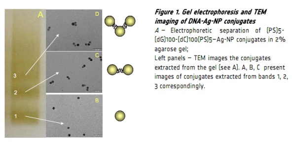
Specific interaction with phosphorothioate residues (PS) was used to connect two silver nanoparticles to
opposite ends of the double stranded DNA. The double stranded poly(dA)-poly(dT) and poly(dG)-poly(dC)
containing 5 PS residues at both 5' ends of these double stranded DNA was synthesized using enzymatic
method developed by us earlier (1). The length of the DNA produced using this method can be varied from
several nanometers up to microns. We have demonstrated that incubation of 100 bp (PS)5-(dG)100-
(dC)100(PS)5 with 15 nm Ag-NPs yielded a mixture of particle monomers, dimers, trimers etc. In the
conjugates each pair of Ag-NPs is bridged by a single DNA molecule. The relative ratio between conjugates
containing different number of particles depends on a particle to DNA molar ratio and can be varied widely.
The individual conjugates can be efficiently separated into discrete bands by the gel (see Fig. 1). The
fractions extracted from the gel slices were further purified by size-exclusion HPLC and visualized by TEM. A
vast majority of molecules in bands 1, 2 and 3 (see Fig. 1 A) correspond to particle monomers, dimers and
timers correspondingly (Fig. 1B, C and D). We performed experiments with shorter poly(dG)-poly(dC), (PS)5-
(dG)30-(dC)30(PS)5 and with poly(dA)-poly(dT) of different lengths and obtained similar results. We have
also demonstrated in preliminary experiments that the particles can also be connected by end-functionalized
parallel stranded G4-DNA structures.
Conductivity measurements of the DNA-NP conjugates are on the way. The conjugates upon the formation
of a bridge between the two metal electrodes will connect them electrically. This will hopefully enable us to
directly measure electrical current trough various DNA structures and to address the issue of charge transfer
in DNA.
[1] Borovok N, Molotsky T, Ghabboun J, Porath D, Kotlyar A. Efficient procedure of preparation and properties of long uniform G4- DNA nanowires. 2008 Anal Biochem. 374, 71-78.
Department of Chemistry, Tsinghua University, Beijing, China, 1000841
E-mail: liudongsheng@mail.tsinghua.edu.cn; Tel.: 86-10-62794081
Based on the i-motif structure, a DNA quadruplex which is formed by DNA containing stretches of cytosine under slight acidic conditions, we have demonstrated a DNA nanomotor driven by pH-change and shown its working ability. We have also employed this DNA nanmotor to fabricate functional devices such as: pH trigged DNA nanocompartment, enthalpy-driven three-State switching of superhydrophilic/ superhydrophobic surface, photo-pH dually modulated fluorescence switch and controllable assembly of gold nanoparticles.1
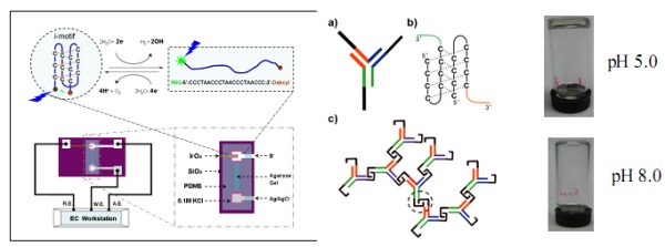
In this talk, we will present our recent studies on DNA motors and smart materials based on i-motif structures. As shown in Figure above (left), using an untraditional three electrodes electrochemical devices, the DNA motor could also be actuated by electric signals. This result will benefit to the integration of DNA motors into conventional silicon based nanodevices for future applications.2 As illustrated in Figure above(right), we have prepared a pH responsive hydrogels entirely made of DNAs. This hydrogel is formed by cross-linking a single type DNA Y-unit building block through the formation of inter-unit i-motif structures. The fast transformation of i-motif has enabled such DNA gel to respond quickly to environmental pH changes to controllably trap and release cargos (i.e. GNPs here) in a pH-dependent manner. In principle, other materials, such as nanoparticles, therapeutic proteins, polymers and even protein producing system could be incorporated into such DNA gel system, allowing the development of functional, responsive biomaterials that have applications in a wide range of disciplines, biosensing, tissue engineering, nano- mechanical devices, and drug delivery etc.3
[1] [1] Liu, H.; Liu, D.; Chem. Commun., 2009, 2625-2636.
[2] Yang, Y.; Fan, C.; Liu, D. et al. Nano Letters 2010, in press.
[3] Enjun Cheng, Dejian Zhou, Dongsheng Liu, et al. Angew. Chem., Int. Ed. 2009, 48, 7660-7663.
CEO, Oxonica Materials Inc., Mountain View, CA U.S.A.
We have developed a series of encapsulated SERS-active labels (SERS nanotags) and several different assay formats that are designed to be used with small or handheld Raman readers for chemical and biochemical sensing applications. We will describe the basic nanomaterials-driven compositions, highlighting the challenges and successes in synthesis, characterization, and scale-up. We will then highlight current applications, ranging from in vivo imaging to ultrasensitive detection of proteins and DNA to detection of low molecular weight species such as aflatoxin and even TNT.
Jozef Stefan Institute, Jamova 39, 1000 Ljubljana, Slovenia
DNA has a valence band composed of nucleobases HOMO orbitals and a conduction band composed of
nucleobases LUMO orbitals. They are separated by an energy gap of ~ 4 eV causing the macromolecule to
be an insulator. In order to improve conducting properties of DNA one should add either additional electrons
in the conducting band or additional holes in the valence band. A possibility of electron doping of DNA
emerged with discovery of M-DNA, a complex which DNA spontaneously forms with transition metal
cations, Co2+, Ni2+ and Zn2+, in buffered water solutions at high pH (= 8.5). The M-DNA complex forms when
divalent metal cations, M2+ replace imino protons, H+ from the hydrogen bonds between complementary
nucleobases in the core of the double helix and bring a net positive charge on the DNA molecule. When the
complex is dried this positive charge cannot be simply neutralized with negative ions on the outer surface
of the double helix and free electrons from the frozen salt matrix must penetrate the double helix to ensure
local charge neutrality.
Here we present spectroscopic measurements on the first example of a chemically electron-doped metal-
DNA complex. We show that a doping level as high as the stoichiometric limit of one electron per base pair
can be achieved in a solid metal-DNA complex Zn-DNA extracted with a freeze-drying method. The doped
unpaired electrons occupy LUMO levels of the nucleobases as detected with Electron Spin Resonance (ESR)
and X-ray Absorption Near Edge Structure (XANES) measurements. Delocalization and strong correlations
between the unpaired electrons are evident from a temperature-independent spin susceptibility and a
microwave (MW) conductivity above 100 K. Below 50 K the unpaired electrons start to localize which is
evident from a sharp decrease in the MW conductivity and a Curie-like increase in the spin susceptibility.
Obviously, the realization of high electron density in the conduction band of DNA by electron doping in the
metal-DNA complex, which is essential for any future application of M-DNA in nanoelectronics, also
introduces the physics of strongly correlated systems into doped DNA systems.
Chemical Nanoscience Laboratory, School of Chemistry, Newcastle University, Newcastle upon Tyne, UK
DNA templated nanowires of pentynyl-modified poly2-(2-thienyl)-pyrrole undergo functionlisation via
metallisation and “click chemistry“. The nanowires retain their 1D-nanostructure and conductive properties
after modification and show promise for incorporation into micro-electrode devices.
Conductive 1D structures, so-called nanowires, are particularly important due to their potential use in
photodetectors, waveguides
and chemical sensors. In the last of these devices advantage is taken of the
highly sensitive nature of the electrical conduction to external pertubations, making them ideal as
transducing elements. A variety of methods for preparing such structures have been developed, including
the use of double helical DNA as a template. This approach has proved quite general and has enabled the
preparation of conducting 1D nanostructures of metals, binary inorganics as well as molecular-based
materials.This is possible because as individual molecules, the strands exhibit extensive non-covalent
interactions with a wide variety of precurors, e.g. metal ions, small molecules, oligomers etc. This ability to
“dope” the biopolymer with these precursors controls the resulting material formation. However, for use as
sensing elements it is not sufficient to produce conducting structures; these must also be capable of
functionalisation with appropriate receptors so as to prime them for capture of a target. Here we report the
preparation of a conducting DNA-based nanowire system that can be readily functionalised. The approach uses
individual strands of DNA to template the growth of a conducting polymer, pentynyl-modified poly-2-(2-thienyl)-pyrrole.
The resulting, supramolecular conductive polymer/DNA hybrid
material is formed as nanowires (step (a) in figure above) which can undergo functionalisation using “click”
chemistry, demonstrated here with a variety of molecular groups (step (b) in figure above). In addition the
terminal alkyne groups strongly influence the subsequent templating reaction of Tollens’ reagent to produce
uniform conductive nanowires comprised of many connected Ag clusters. We confirm that the nanowires
are electrically conducting before and after these processes using a range of probe microscopy techniques.
1- The Hebrew University of Jerusalem, Israel 2-Tel Aviv University, Israel, 3-INFM-Modena Corresponding author: porath@chem.ch.huji.ac.il
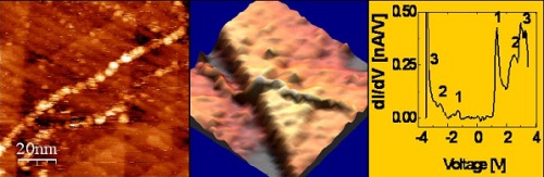
STM and STS of poly(G)-poly(C) DNA. (a) Topography image of the DNA on Gold (b). 3D presentation of the same image (c) STS on the molecule.
DNA has been in the center of the scientific research for decades. In particular, DNA was considered as one
of the attractive candidates for molecular electronics. Attempts to resolve the energy level structure of
single DNA molecules span over the last two decades, thanks to the unique ability of scanning tunneling
spectroscopy (STS) to probe the local density of states of deposited objects. Nevertheless, success was
hindered by extreme technical difficulties in stable deposition and reproducibility. By measuring STS on DNA
at cryogenic temperature, for the first time we disclosed the energy spectrum of poly(G)-poly(C) DNA and
G4-DNA molecules deposited on gold. The tunneling current-voltage (I-V) characteristics and their
derivatives (dI/dV-V) exhibit a clear gap and a peak structure around the gap. Fluctuations in the I-V curves
are observed and statistically characterized. The character of the observed dI/dV-V peaks is assigned to
orbitals originating from the different molecular components, namely the nucleobases, the backbone and the
counterions, by means of ab initio Density Functional Theory calculations.
As time allows, I will show a selection of the following topics from our research: (i) Progress in electrical
transport measurements. (ii) Comparison of polarizability between G4-DNA variants.
[1] “Direct Measurement of Electrical Transport Through Single DNA Molecules of Complex Sequence”, Hezy Cohen, Claude Nogues,
Ron Naaman and Danny Porath, PNAS 102, 11589 (2005).
[2] "Long Monomolecular Guanine-Based Nanowires." Kotlyar, A. B., Borovok, N., Molotsky, T., Cohen, H., Shapir, E. & Porath, D. Adv.
Mater. 17, 1901 (2005).
[3] “Electrical characterization of self-assembled single- and double-stranded DNA monolayers using conductive AFM”, Hezy Cohen
et al., Faraday Discussions 131, 367 (2006).
[4] “Long Monomolecular G4-DNA Nanowires”, Alexander Kotlyar, Nataly Borovok, Tatiana Molotsky, Hezy Cohen, Errez Shapir and
Danny Porath, Advanced Materials 17, 1901 (2005).
[5] "Polarizability of G4-DNA Observed by Electrostatic Force Microscopy Measurements", Hezy Cohen Hezy Cohen et al., Nano
Letters 7(4), 981 (2007).
[6] “High-Resolution STM Imaging of Novel Poly(G)-Poly(C)DNA Molecules”, Errez Shapir, Hezy Cohen, Natalia Borovok, Alexander B.
Kotlyar and Danny Porath, J. Phys. Chem. B 110, 4430 (2006).
Institute of Nanoscience of CNR, National Nanotechnology Laboratory- Lecce
University of Salento,Via Arnesano 16, 73100 Lecce, Italy
Ross.rinaldi@unisalento.it
www.nnl.it
Recently we developed several nano-biotechnological approaches aimed at the realization of arrays of biomolecules (arrays of DNA, proteins, antibodies) with micro- or nanoscale spatial resolution. Surface chemistry procedures were combined with lithographic techniques for the realization of nanostructured substrates with biorecognition capability, and the various processes were optimized in order to obtain highly uniform and functional immobilized biomolecules (for instance, retention of the native folding of fluorescent proteins). Moreover, based on the covalent immobilization of stable and versatile SAMs of programmable chemical reactivity, this approach constitutes a general platform for the parallel site-specific deposition of a wide range of molecules, such as organic fluorophores and water soluble colloidal nanocrystals. Notably, we developed versatile strategies compatible with the use of a wide range of different materials (e.g., plastic materials, glass, quartz, silica) of great interest for the realization of biochips for analytical and diagnostic applications. In this talk I will present some possible approaches for the implementation of biosensors and Lab-on-chip devices, based on polymeric materials, exploiting membrane receptors, hybrid systems, colloidal semiconductor nanocrystals (NCs), novel materials and interfaces and different fluorescence or electrical sensing schemes, for highly sensitive real-time analyses of biomolecules. I will also show some recent strategies for the development of cell chips for diagnostic and drug screening based on different detection methods for real-time monitoring of morphological changes and/or of specific cellular processes.
¹ Lausitz University of Applied Sciences, Senftenberg, Germany; 2 Attomol GmbH, Lipten, Germany; 3 GA Generic Assays GmbH, Dahlewitz, Germany; 4 PolyAn GmbH, Berlin, Germany
There is an increasing demand for multiplex techniques enabling the simultaneous assessment of multiple
biomolecules in one biological sample in research and clinical diagnostics. Due to their high flexibility
microbead-based multiplex detection systems close a gap between single and high-throughput detection
methods.
Within the framework of the InnoProfile project “Real-time-PCR-Array“ we developed a microbead-based
multiplex antibody and DNA detection technology. Main pillars for this technology are A) Fluorescent
microbead populations which are defined by varying ratios of two fluorophores and B) The multi-fluorescent
color detection platform VideoScan with novel pattern-recognition algorithms.
A) Microbeads: Proteins for the detection of antibodies or oligonucleotide capture probes for the detection of
PCR products are coupled on microbeads. Specific antibodies bind to microbead-coupled antigens and are
detected by a fluorescence-labeled secondary antibody. PCR products are fluorescence-labeled during the
PCR reaction and hybridize to microbead-coupled capture probes. Binding of fluorescence-labeled secondary
antibodies or PCR products results in a specific fluorescence corona around a microbead. The intensity of a
fluorescence signal correlates with quantities of bound antibodies or PCR products. Fluorescence corona and
affiliation of one microbead to one of 18 microbead populations are automatically analyzed by the VideoScan
platform. Size, surface, thermostability and degree of carboxylation of microbeads as well as photostability
of fluorophores determine efficiency and robustness of the interpretation process.
B) The VideoScan platform is a flexible imaging technology with a broad spectrum of applications such as I)
Protein and DNA quantification due to fluorescence signals on microbead surfaces, II) Cell- and tissue-
based immunofluorescence assays, III) Bacterial adhesion and invasion assays by the detection and
quantification of fluorescent bacteria. The VideoScan platform is based on automatic capturing and
processing of two-dimensional images and consists of the following main components: motorized inverse
microscope with three fluorescence channels, motorized scan-stage, digital grey-scale camera and computer
running software for controlling and processing.
The VideoScan is a flexible and automatic multi-parametric analysis system with a great potential for
further diagnostic and biochemical applications.
Center for Functional Nanomaterials, Brookhaven National Laboratory, Upton, NY 11973-5000, USA; wsherman@bnl.gov
Branched DNA can be used to create structures with feature sizes significantly smaller than are accessible via photolithography. There is great potential utility in learning how to attach functional guests onto DNA nanostructures in such a manner that the guests can be organized with a level of structural precision comparable to that of the DNA scaffold. Gold Nano-Particles (AuNPs), have been the prototypical targets for this undertaking, largely because their electrical and optical properties are strongly dependent on their diameter. Unfortunately, branched DNA nanostructures will generally only form in a buffer solution that has approximately a 10 mM concentration of divalent counter ions – typically Mg2+. AuNPs, on the other hand, tend to aggregate rapidly in such solutions, which limits their availability for attaching to DNA scaffolds. We have found that AuNPs that have both DNA strands and zwitterions attached to their surfaces can resist aggregation in the typical buffers used for DNA nanostructure assembly; further, the DNA on the NPs retains its availability for hybridization. We have built a two dimensional scaffold of triangular units that does not form in the absence of Mg2+ ions. The scaffold has spaced triplets of sticky ends that serve as attachment points for AuNPs. The connections between the scaffold and the AuNPs include both flexible, single- stranded DNA and relatively rigid double helices. With the proper lengths of flexible and rigid linker segments, triplets of binding sites on a single triangle are occupied by single AuNPs, as can be observed via scanning electron microscopy.
Contrast enhanced scanning electron micrographs of 5 nm diameter gold nanoparticles. A) The AuNPs in the absence of the DNA scaffold, organized by capillary forces during drying. The average center-to-center particle spacing is ~12 nm. B) Similar particles arranged on a DNA scaffold (not visible). The average spacing is approximately the expected 28 nm.
Harvard Medical School, Department of Cancer Biology
Dana-Farber Cancer Institute, 44 Binney St., Boston, MA 02115
Contact: William_Shih@dfci.harvard.edu
I will present a general method for solving a key challenge for nanotechnology: programmable self- assembly of complex, three-dimensional nanostructures. Previously, scaffolded DNA origami had been used to build arbitrary flat shapes 100 nm in diameter and almost twice the mass of a ribosome. We have succeeded in building custom three-dimensional structures that can be conceived as stacks of nearly flat layers of DNA. Successful extension from two-dimensions to three-dimensions in this way depended critically on calibration of folding conditions. We also have explored how targeted insertions and deletions of base pairs can cause our DNA bundles to develop twist of either handedness or to curve. The degree of curvature could be quantitatively controlled, and a radius of curvature as tight as 6 nanometers was achieved. This general capability for building complex, three-dimensional nanostructures will pave the way for the manufacture of sophisticated devices bearing features on the nanometer scale.
1 Jenaer Biochip Initiative, Friedrich-Schiller-University Jena, Institute of Physical Chemistry, Helmholtzweg 4, Jena, Germany
2IPHT - Institute of Photonic Technology, Albert-Einstein-Straße 9, 07745 Jena, Germany
Surface enhanced Raman spectroscopy (SERS) is an emerging technology in the field of analytics. Due to the
high sensitivity in connection with specific molecular fingerprint information SERS can be used in a variety
of analytical, bioanalytical, and biosensing applications. SERS could also be used for a chip based detection
of biologically active molecules and low molecular substances. However, for the SERS effect, substrates
with metal nanostructures are needed. The broad application of this technology is greatly hampered by the
lack of reliable and reproducible substrates. To use SERS as standard analytical tool cheap and reproducible
substrates are required.
Here we highlight an alternative approach to produce low cost and reproducible substrates for SERS
applications, which allows a simple, economical and highly space-resolved production. The fabrication
process is based on an enzyme induced deposition of silver nanoparticles. The special structural feature of
the enzymatically generated silver nanoparticles allows their application for a variety of excitation
frequencies in the visible and NIR region. Furthermore, the exceptional morphology of the SERS substrate
enables a qualitative and semi quantitative statement of the SERS activity due to a simple measurement of
the DC conductivity measurement.
These novel SERS substrates of enzymatically generated silver nanoparticles were used for the qualitative
and quantitative chip based detection of low molecular substances like dyes and antibiotics. Furthermore,
due to the combination of SERS and magnetic nanoparticles, a sequence specific detection of DNA of
epizootic disease causing pathogens was realized. Here we will present our first results on this
bioanalytical system. In first experiments we investigate the applicability of our system with short
synthetic oligonucleotides and evaluate the specificity. Furthermore we transfer this system to DNA strands
that were amplified via PCR, which is closer to reality than short synthetic oligonucleotides. As PCR targets
sequences of the bacterium Mycoplasma mycoides subspecies mycoides small colony type (MmmSC), which
causes the epizootic disease contagious bovine pleuropneumonia (CBPP) were used. In the end we will
display the potential of this bioanalytical system for the analysis of PCR product and native ssDNA.
Acknowledgement Funding of research projects “Jenaer Biochip Initiative (JBCI)” within the framework “Unternehmen Region – Inno Profile” and ATLAS from the Federal Ministry of Education and Research, Germany (BMBF) is gratefully acknowledged. K. Weber gratefully acknowledges financially support by “Carl-Zeiss-Stiftung”.
1Nanoscience Center, Department of Physics, P.O. Box 35, FI-40014 University of Jyväskylä, Finland
2Department of Applied Physics, P.O. Box 5100, FI-02015 Helsinki University of Technology, Finland
Controlled positioning and immobilization of DNA molecules and structures on the chip is a crucial open
challenge for the realization of the full potential of the bottom-up DNA-nanotechnology, and to further study
such systems. Dielectrophoresis (DEP) can be used to trap DNA molecules and self-assembled structures,
such as DNA origami [1] which is a striking example of an efficient DNA bottom-up technique. The optimized
DEP-method gives a high yield of single structure trapping between nanoelectrodes, and thus provides
controlled positioning of the structures on a chip and means of bridging bottom-up and top-down
fabrication approaches.
In this study we have utilised DEP to trap DNA origami structures, and after the immobilization of an
individual DNA structure between the nanoelectrodes, the electrical conductivity of the structure was
characterized. We have fully analyzed both DC and AC characteristics (AC impedance spectroscopy) of single
trapped rectangular DNA origami structures within environments with different humidity levels, and also
defined the detailed equivalent circuit model describing the conductivity mechanism of the structure [2]. The
results revealed that the nature of the conductivity is not purely Ohmic but that it is a combination of an
ionic diffusion and electronic conductivity. Also other kinds of selfassembled DNA structures are being
measured and analyzed with the same method.
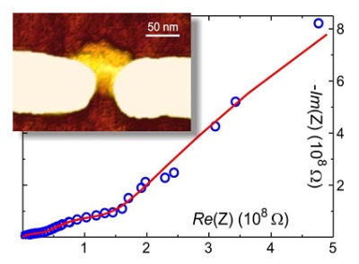
Figure. Inset: AFM Image of a rectangular DNA origami trapped and immobilized between nanoelectrodes. Graph: AC impedance spectroscopy data measured from the structure (circles) and the response of a fitted equivalent circuit (line).
[1] A. Kuzyk, B. Yurke, J.J. Toppari, V. Linko, and P. Törmä, Small 4(4) (2008) 447. [2] V. Linko, S.-T. Paasonen, A. Kuzyk, P. Törmä, and J.J. Toppari, Small 5(21) (2009) 2382.
Aalto University School of Science and Technology v
We consider two different topics. The first one is related to the interaction of organic molecules with
surface plasmon polaritons (SPP), i.e. electro-magnetic fields confined within nanoscale dimensions near a
metal surface. We present the observation of a large room-temperature vacuum Rabi splitting [1] for SPP
and dye molecules, paving the way for the use of strong coupling phenomena in a variety of molecular
plasmonics systems.
The second topic concerns DNA origami, a method of creating complicated nanoscale shapes out of DNA
using its self-assembly properties. We show how DNA origami structures can be positioned on chip using
dielectrophoresis [2], and how they can be used as a nanobreadboard to assemble complicated patterns
with below 10 nm resolution [3]. We also discuss recent work on combining our carbon nanotube [4] and
DNA-related research.
[1] T.K. Hakala, J.J. Toppari, A. Kuzyk, M. Pettersson, H. Tikkanen, H. Kunttu, and P. Törmä, Vacuum Rabi splitting and strong
coupling dynamics for surface plasmon polaritons and Rhodamine 6G molecules, Phys. Rev. Lett. 103, 053602 (2009).
[2] A. Kuzyk, B. Yurke, J.J. Toppari, V. Linko, and P. Törmä, Dielectrophoretic trapping of DNA origami, Small 4, 447 (2008).
[3] A. Kuzyk, K.T. Laitinen, and P. Törmä, DNA origami as a nanoscale template for protein assembly, Nanotechnology 20, 235305
(2009).
[4] M. Rinkiö, A. Johansson, G-S. Paraoanu, and P. Törmä, High speed memory from carbon nanotube field-effect transistors with
high-? gate dielectric, Nano Lett. 9, 643 (2009).
Institute of Chemistry, The Hebrew University of Jerusalem, Jerusalem 91904, Israel E-mail: willnea@vms.huji.ac.il
The information encoded in the base sequence of the nucleic acids provides instructive information for the
self-assembly of supramolecular nanostructures exhibiting programmable topological properties, recognition
and catalytic functions, and molecular machinery operations. These different topics will be addressed with
the following examples:
- Nucleic acids exhibiting tailored complementarities or carrying appropriate chemical functionalities
self-assemble into catenated DNA chains, hexagonic strips, graphitic-type nanotubes, and covalently linked
nanotubes. The nanostructures enable the programmed addressing of proteins and the activation of
enzyme cascades, and they act as nano-containers for metal/semiconductor nanoparticles.
- Different DNA machines that function as a "bipedal walker", "gear", molecular "seesaw", molecular
"crane", and three coherent "tweezers" will be introduced. The significance of these structures as nano-
transporters, controlled release systems and biomolecular computing will be discussed.
- The self-assembly of nucleic acids into supramolecular structures exhibiting tailored recognition
properties (aptamers) or catalytic functions (DNAzymes) will be presented. The use of the systems for
amplified sensing, and particularly, as isothermal self-replicating systems, will be introduced.
- The functionalization of semiconductor quantum dots (QDs) with metal-porphyrin/G-quadruplex
structures will be described, and the utilization of the systems for optical sensing and photocatalysis will be
introduced.
Institute of Photonic Technology, Albert-Einstein-Str. 9, 07745 Jena, Germany
The manipulation of biological molecules at the nanometer scale by means of ultrashort laser pulses shows great promise for applications in molecular medicine. Because of their unique optical properties, like the plasmon resonance, noble metal nanoparticles can act as laser light antennas and allow a very local energy conversion of laser pulses from the nanoparticle into the surrounding medium [1, 2]. In this talk, we present experiments of the energy conversion from metal nanoparticles into double stranded DNA molecules induced by laser light. After the silver nanoparticles were bound to DNA, the DNA was immobilized on a thermo- and electron sensitive layer (polymethylmethacrylate, PMMA) and irradiated by laser light at a wavelength of 800 nm. The influences of the excited nanoparticles on the DNA-molecules were characterized by atomic force microscopy.
[1] Garwe, F., Bauerschafer, U., Csaki, A., Steinbruck, A., Ritter, K., Bochmann, A., Bergmann, J., Weise, A., Akimov, D., Maubach, G.,
Konig, K., Huttmann, G., Paa, W., Popp, J. and Fritzsche, W. (2008) Optically controlled thermal management on the nanometer
length scale. Nanotechnology, 055207
[2] Csaki, A., Garwe, F., Steinbruck, A., Maubach, G., Festag, G., Weise, A., Riemann, I., Konig, K. and Fritzsche, W. (2007) A Parallel
Approach for Subwavelength Molecular Surgery Using Gene-Specific Positioned Metal Nanoparticles as Laser Light Antennas.
Nano Lett. 7, 247 - 253
Department of Chemistry and Biochemistry, Brigham Young University, Provo, Utah, USA http://people.chem.byu.edu/awoolley
We are utilizing DNA to form nanometer-scale structures1 with potential for application as integrated circuit templates. Using DNA origami2 we have constructed nanoscale objects having a range of sizes and shapes.3 Importantly, our DNA nanostructures contain multiple branching points, have asymmetric junctions, and feature linewidths of about 10 nm (see Figure 1), all desirable properties for forming nanoelectronic components. We are optimizing procedures for selectively seeding and plating DNA origami. Our present efforts focus on the formation of three-dimensional DNA origami constructs for nanoelectronics applications and the controlled assembly of DNA origami into periodic arrays. This work showcases the considerable capabilities of DNA for bottom-up self-assembly of nanoscale features.
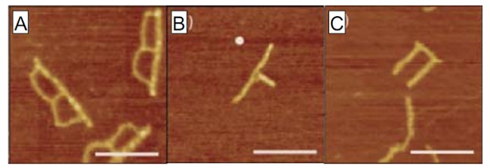
Figure 1. Atomic force microscopy characterization of thin, branched DNA origami structures. (A) “B” shape. (B) “Y” shape. (C) “U” shape. Scale bars are 200 nm.
[1] Becerril, H.A.; Woolley, A.T. DNA-Templated Nanofabrication. Chem. Soc. Rev. 38, 329-337 (2009).
[2] Rothemund, P.W.K. Folding DNA to Create Nanoscale Shapes and Patterns. Nature 440 297-302 (2006).
[3] Pound, E.; Ashton, J.R.; Becerril, H.A.; Woolley, A.T. PCR-based Scaffold Preparation for the Production of Thin, Branched DNA
Origami Nanostructures of Arbitrary Sizes. Nano Lett. 9, 4302-4305 (2009).
University of Toronto;
Senior Scientist, Tanenbaum Chair in Prostate Cancer Research
Ontario Cancer Institute, TMDT 5-363, 101 College St, Toronto, ON M5G 1L7
Contact : gang.zheng@uhnres.utoronto.ca
The emerging field of nanophotonics has created a diverse set of novel tools and opportunities for biological sensing, optical imaging and photonics-based therapy (e.g., photodynamic therapy and photothermal therapy). Compared with their well documented impact on in vitro clinical diagnosis and biomarker discovery, nanophotonics’ translation into clinical viable tools for in vivo imaging and therapy is slowed by many formidable hurdles (e.g., delivery to the correct cells/tissues at a level that is safe for patients). Three lipid-based nanophotonics platform technologies will be introduced here with the goal of addressing some of these translation hurdles. First, we created a metal free phototransducing lipid nanovesicle that combines the powerful phototransucing properties (e.g., photothermal, photoacoustic) of gold nanoparticles and the natural biocompatibility and superior drug carrying capability of liposomes. Such ‘phototransducing liposomes’ could transform traditional organic drug nancarriers into versatile biophotonic tools. Secondly, by mimicking the assembly and functions of natural lipoproteins, we created several classes of lipid nanoparticles suitable for the systematic targeted delivery of photodiagnostic and therapeutic agents to cancer cells. These spherical and small (<40nm) nanostructures are designed for optimizing the nanoparticle tumor penetration and the intracellular probe delivery. In the third platform, we integrated the classic hairpin molecular beacon concept into lipid nanostructures and created a powerful nucleic acid sequence- controlled lipid nanoparticle aggregation strategy that has a number of potential utilities for in vivo biosensing and imaging.
1 Department of Complex Matter, J. Stefan Institute, Jamova 39, 1000 Ljubljana, Slovenia; Telephone: +38614773342, Fax: +38614773998; Email: miha.devetak@ijs.si
2Dipartimento di Chimica Organica “A. Mangini”, Alma Mater Studiorum - Università di Bologna, via San Giacomo 11, 40126 Bologna, Italy;
3Faculty of Mathematics and Physics, University of Ljubljana, Jadranska 19, 1000 Ljubljana, Slovenia;
We studied surface organization of lipophilic guanosine derivatives with one, two and three alkanoyl tails in
thin films on water surface and in Langmuir-Blodgett (LB) films transferred onto freshly cleaved mica
substrate. The derivative with one alkanoyl group exhibits irreversible pressure-area isotherms and ribbon-
ike LB film structures. The derivatives with two and three side groups show reversible isotherms with
similar critical surface pressures, whilst their LB film structures are quite different. The derivative with two
tails forms films with flat terraces of micrometer size, while the derivative with three tails exhibits irregular
thread-shaped assemblies. These observations demonstrate that molecular assembly of LB films of
guanosine derivatives can be effectively manipulated by altering the number of attached lipophilic groups.
From the point of view of nanotechnology, the material with two tails (dG(C10)2) seems to be the most
promising for applications requiring homogeneous films with well defined and tunable thickness. Our
preliminary investigations of multilayer LB films of this derivative showed that regular terrace-like
morphology is preserved also in multilayer structures. The derivative with three tails (G(C10)3) is likely
unsuitable for applications, as its LB film structures are very irregular and practically cannot be controlled.
The ribbon-like LB film structure of the derivative with one tail (GACE(C10)) is promising for applications
requiring 1D building blocks. Its properties might be further improved by developing appropriate methods
leading to alignment of the ribbons along a predetermined direction. In addition to this, intermolecular
hydrogen bonding, which might occur in Langmuir films of this derivative, provides additional possibility for
tuning the properties of its LB film structures. The tuning can be achieved either via adding assembly
stimulating ions to the water subphase or by dilution of the material with some other lipophilic molecules.
The arrangements of the molecules on surface can be studied by a Langer-Blodgett technique, Atomic force
microscopy and Sum-frequency generation nonlinear optical method.
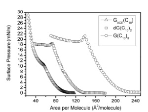
Figure 1: Surface pressure versus area isotherms of Langmuir films of GACE(C10), dG(C10)2 and G(C10)3 on water subphase.
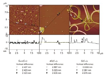
Figure 2: AFM images of LB films of GACE(C10) (left), dG(C10)2 (middle), and G(C10)3 (right) deposited on muscovite mica. Vertical cross sections along the marked lines are reported below each image. The values displayed at the bottom are vertical distances between the markers of the same colour.
[1] Devetak et al., Surface structure of Langmuir-Blodgett films of lipophilic guanosine derivatives, Applied Surface Science 256, 7,
(2010) 2038-2043.
[2] Kunstelj et al., Self-organization of guanosine 5’-monophosphate on mica, Coll.Surf. B: Biointerfaces 59 (2007) 120-127.
1Aalto University, Department of Applied Physics, P.O. Box 11000, FI-00076 AALTO Finland email: anteske@cc.hut.fi 2Nanoscience Center, Department of Physics University of Jyväskylä P.O. Box 35, FI-40014 Finland
While self-assembly has proven its usefulness for the generation of various nano- and mesoscopic structures, there remains a fundamental obstacle in creating integrated, highly ordered multicomponent nanodevices: the precise spatial control over each of the device components has proven to be exceedingly difficult. Here, a high-precision, high-throughput method for pattern transfer of nano-objects is demonstrated by producing arrays of quantum dots [1]. The method, field-induced nanolithography (FINAL), utilizes dielectrophoresis for trapping and it can be extended to arranging carbon nanotubes, biomolecules, and other objects into desired configurations. The trapping as well as the subsequent deposition from the master stamp to the target plate are made in parallel fashion, enabling large area printing and mass production. Furthermore, the master stamp is i) reusable, and ii) more importantly and in contrast to conventional methods such as microcontact printing and nanoimprint lithography, universal: one master stamp having a 2D matrix of electrodes could be used to transfer any desired pattern to the target plate. Due to its robustness, versatility, and universality, the method has remarkable application potential in nanotechnology.
[1] T. K. Hakala, V. Linko, A.-P. Eskelinen, J. J. Toppari, A. Kuzyk, and P. Törmä, Small 5 (2009) 2683-2686.
1Department of Applied Physics, Aalto University School of Science and Technology, Finland
2Physics Department, Technical University Munich, Germany
marcus.rinkio@phys.jyu.fi
DNA has a superior self-assembly properties, which have been utilized in many nanoscience applications Maybe the most prominent examples are the different variations of origami structures constructed from DNA, including 2D structures of arbitrary shapes1,2 and even 3D structures with functionality3,4. We would like to use the DNA origami as a template for structured molecule attachment for self-assembled electronics.
[1] Rothemund, P.W.K. Folding DNA to create nanoscale shapes and patterns. Nature 440, 297-302 (2006).
[2] Andersen, E.S. et al. DNA Origami Design of Dolphin-Shaped Structures with Flexible Tails. ACS Nano 2, 1213-1218 (2008).
[3] Andersen, E.S. et al. Self-assembly of a nanoscale DNA box with a controllable lid. Nature 459, 73-76 (2009).
[4] Douglas, S.M. et al. Self-assembly of DNA into nanoscale three-dimensional shapes. Nature 459, 414-418 (2009).
Walter Schottky Institut (WSI), Technische Universität München,
Am Coulombwall 3, 85748 Garching
We investigate the dynamics of electrically actuated DNA layers which are attached to a gold surface. The DNA conformation on the surface is modulated (switched) by electric fields due to the intrinsic charge of the DNA backbone. The fluorescence signal of a dye at the distal end of the DNA strand is used to monitor the conformation change, as the apparent quantum yield depends strongly on the distance between the dye and the metal surface. The modulation efficiency of our layers is affected by the salt concentration in buffer solution due to counter ion screening at the metal/solution interface and the molecular dynamics of the DNA switching are found to depend on the charging properties of this electrochemical double layer. A novel method to perform time resolved measurements allows us to monitor the individual upward and downward motions of the electrically driven DNA motion on a sub?microsecond timescale. We determine the dynamic properties of the system by evaluation of the characteristic rise and fall times. Employing the time resolved method, influences of the DNA surface density and the DNA length on these time constants are studied. The introduced methods are then applied to monitor the binding of proteins (target) to DNA layers (probe) and to study the dynamics of electrically actuated DNA?protein conjugates. IgG antibodies and antibody fragments are bound to the DNA layer and the influence of the attached proteins on the DNA dynamics are studied. As the bound proteins increase the hydrodynamic drag and thus the rise time of the DNA probe, we can infer the size of the proteins from an analysis of the switching dynamics of the DNA?protein conjugate.
Institut Charles Delaunay, Université de Technologie de Troyes, CNRS FRE 2848, Laboratoire de Nanotechnologie et d’Instrumentation Optique 12, rue Marie Curie, BP-2060, F-10010 Troyes Cedex, France
The electrical properties of nanowires are influenced by minor perturbations to the surrounding environmen because of their high surface-to-volume ratio and small size.[1] When functionalized with appropriat ‘capture probes’ and integrated into electronic devices, nanowires can act as transducers for label-fre electrical detection of a variety of chemical and biological species.[2,3] DNA templating provides a practica and reproducible route to nanowire formation that has been shown to be compatible with a wide variety o materials.[4] Current work focusing on DNA-based nanowires of thienyl-pyrrole derivatives with alkyny groups is presented. FTIR data demonstrates the availability of the alkyne group for subsequent nanowir functionalisation using ‘click’ chemistry. Atomic Force Microscopy (AFM) shows well aligned DNA-template nanowires on SiO2 substrates (see Figure), while electrical characterization using methods such as Scanne Conductance Microscopy (SCM) confirm the conducting nature of these nanomaterials.
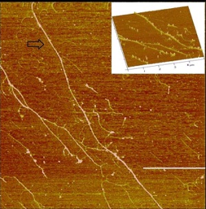
Figure: Black arrow: DNA/pentnyl-TP ~5-6 nm in height stretched on silanized silicon (111) surface, the scale bar = 3 µm and the height scale is 10 nm.
[1] Lutz, Jean-Francois. et al. (2008), Prog. Polym., Sci. 33, 1-39.
[2] Yogeswaran, U. (2008), Sensors, 8, 290-313.
[3] Lange, U. et al. (2008), Analytica Chimica acta, 614, 1-26.
[4] Houlton et al. (2009), Chem. Comm., 1797-1806.
1Institute of Photonic Technology, Albert-Einstein-Straße 9, 07745 Jena
2Julius Kühn-Institute, Messeweg 11/12, 38104 Braunschweig
3Institute for Physical Chemistry, Friedrich-Schiller-University Jena, Helmholzweg 4, 07743 Jena
Phytophthora [1] is a genera of fungal-like plant parasitic pathogens that causes commercially severe plant
losses worldwide. The most famous example is the Great Famine in Ireland mid of the nineteenth century.
It was caused by P. infestans the causal agent of the late blight of potato. Today the most dangerous
Phytophthora species are regulated, some as quarantine organisms [www.eppo.org] like P. ramorum [2] the
causal agent of Sudden Oak Death in the natural habitats along the Californian coast side in the USA
[www.suddenoakdeath.org]. To prevent the spread of these pathogens, plants and plant products must be
examined before they are sold or exported. Furthermore there are strict regulations for plant control at the
boarders. Therefore the plant protection services and the plant inspectors ask for highly specific, sensitive
and easy to handle diagnostic methods, which give results within short time.
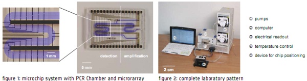
We demonstrate a lab-on-a-chip system for rapid nucleic acid-based analysis within approx. 3 hours that
can be applied for diagnosis of Phytophthora. This microchip system integrates a PCR-chamber for
amplification and labelling of nucleic acids and microarray technology for sequence specific analysis within a
single platform (fig. 1). All necessary reaction steps can be performed consecutively within a single chip with
integrated microchannels and microchambers. The microarray is read out by a simple electrical
measurement. To enable the electrical readout all spots are placed in electrode gaps. In case of successful
hybridisation, elementary silver can be deposited by an enzymatically catalysed reaction. If so the gaps will
be closed and electrical conductivity can be measured [3]. Temperature management of PCR- and
hybridisation-zone is realised by two independent Peltier elements. The chip will be integrated in a compact
portable system with a pump and power supply so the development of a point of care device is possible
(fig. 2).
Because of its universal character this lab-on-a-chip system is open for other applications such as
qualitative diagnosis of infectious or hereditary diseases based on specific nucleic acid sequences.
Funding by the Federal Agency for Agriculture and Food (BLE) is acknowledged (FKZ: 28-1-42.028-06).
[1] Erwin D. C. and O.K. Ribeiro, Phytophthora Diseases Worldwide. The American Phytopathological Society, St. Paul, Minnesota,
1996, pp. 562
[2] Werres, S., et al., Phytophthora ramorum sp. nov., a new pathogen on Rhododendron and Viburnum. Mycol Res, 2001. 105(10):
p. 1155-1165.
[3] Möller, R., et al., Electrical DNA-chip-based identification of different species of the genus Kitasatospora. Appl Microbiol
Biotechnol, 2008. 77(5): p. 1181-1188.
1Department of Applied Physics, Aalto University School of Science and Technology, P.O. Box 15100, FI- 00076 AALTO, Finland.
2Physics Department E14, Technical University of Munich, James-Franck-Strasse 1, D-85748 Garching, Germany.
33Nanoscience Center, Department of Physics, University of Jyväskylä P.O. Box 35, FI-40014, Finland.
†Present address.
email: anton.kuzyk@ph.tum.de
Due to its exceptional self-assembly properties, DNA could become a key player in bottom-up fabrication of nanoscale systems.1 A striking example of a DNA self-assembly technique is “DNA origami“ which involves folding of long single-stranded DNA with the help of short oligonucleotides.2 DNA molecules and DNA self- assembled structures can be used as a template for attachment of various materials (proteins, carbon nanotubes, nanoparticles etc). In case of DNA origami each short oligo can serve as a pixel. Therefore, origami structures can be decorated with complex patterns with below 10 nm resolution. Ability to control relative position of molecules with nanometer precision is of extreme importance for understanding fundamental biomolecular interactions, e.g. of enzymes. Recently we have demonstrated that DNA origami structures can be used for assembly of complex proteins patterns.3 Similar approach can be used for assembly of enzymes and carbon nanotubes. To realize the full potential of DNA origami as a template, we have developed dielectrophoresis based method for controlled trapping of origami structures between nanoelectrodes.4Such trapping is the first demonstration of the dielectrophoretic manipulation of complex self-assembled structures and is an example of successful combination of bottom-up and top-down fabrication approaches.
[1] N. C. Seeman, Nature 421 (2003) 427.
T. H. LaBean and H. Li, Nano Today 2 (2007) 26.
[2] P. W. K. Rothemund, Nature 440 (2006) 297
[3] A. Kuzyk, K. T. Laitinen, P.Törmä, Nanotechnology 20 (2009) 235305.
[4] A. Kuzyk, B. Yurke, J. J. Toppari, V. Linko, P. Törmä, Small 4 (2008) 447.
Institute of Photonic Technology (IPHT) Jena, PO Box 100239, 07745 Jena, Germany
Dielectrophoresis (DEP) is a suitable method for the microintegration of bottom-up nanoscale structures in an existing top-down microelectronic environment. This technique is based on the moving of polarizable objects under the influence of an AC-field. In combination with real-time microscopy the characterization and investigation of the DEP parameters for nanoscale objects can be achieved. By ajusting of different process parameters for every nanostructure or biospecies it is possible to influence orientation and integration geometry between microelectrodes. This integration principle offers a great potential for nanophotonics, nanoelectronics and on-chip applications. It was possible to direct cells, form conductive nanoscale bridges between two electrodes and stretch DNA-based structures between electrodes. Furthermore, integration of nanosized structures e.g. nanoparticles and nanowires could be also demonstrated. Current developments are focused on the investigation of the sensoric potential of defined integrated nanostuctures for bioanalytical applications.
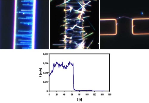
Figure 1) Microintegrated nanoparticles (top, left), nanowires (top, middle), defined nanoparticle bridge (top, right) and sensoric measurement on nanoparticle bridge (bottom).
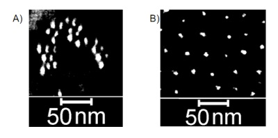
1Department of Biochemistry, George S. Wise Faculty of Life Sciences, Tel Aviv University, Ramat Aviv, 69978 Israel
2Nanotechnology Center, Tel Aviv University, Ramat Aviv, 69978 Israel
It is known that guanines, which have the lowest ionization potential among DNA bases, promoting charge
migration through the DNA. These properties make G-quadruplexes very promising for nanoelectronic.
Experimental studies showed that that G-quadruplexes are characterized by a clear polarizability, which is
indicative of possible electrical conductivity.
Direct measurement of the DNA conductivity is a very challenging task due to multiple reasons. One of them
is the inability to efficiently transfer current through G4-DNA molecules deposited in-between metal
electrodes with poor electrical contact between the DNA and the electrode surface. In order to overcome
this problem and to promote an electric communication between the G4-DNA and the electrodes we
decided to use G4-DNA-AgNP conjugates schematically presented in Figure 1A. As seen in the figure the
two particles are connected to one another though a parallel stranded G-quadruplex molecule. The G4-DNA
structures were prepared using a 5'-aaaaa(20G)aaaaa-3' oligonucleotide, containing 20G in the middle of
the strand and 5 phosporithioate A bases (a) at its 3' and 5'-ends and 15 nm silver nanoparticles (AgNP).
The strands were assembled at high oligonucleotide concentrations (>0.5 mM) in the absence of K and Na.
Incubation of the strands in these conditions yields individual G4 molecules and not long G-wires composed
of a large number of annealed oligonucleotides. We have shown that the CD spectrum of the structures is
similar to that reported for four stranded G-quadruplexes. We have also demonstrated that the structures
are uniform and migrate as a single band during electrophoresis. The phosporithioate fragments on both
side of the G-quadruplex bind covalently to the surface of silver particles linking them together into a dimer
(see Fig. 1A). Incubation of AgNPs with three-four molar excess of the end-functionalized G-quadruplexes
lead to the formation of short chains of the particles (see Fig 1B) in which the two neighboring particles are
connected by the G-quadruplex. Electrical measurements of these structures, we believe, will provide new
insights into the mechanism of DNA conductivity.
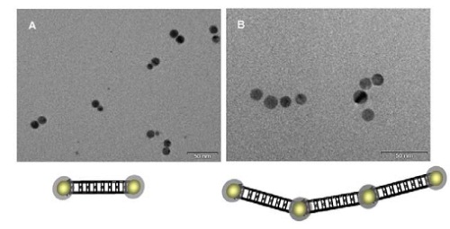
Figure1. TEM images of AgNP dimers (A) and short chains of AgNP (B) connected by G4-DNA
Institute of Photonic Technology, Albert-Einstein-Str. 9, 07745 Jena, Germany * Aalto University School of Science and Technology, P.O.Box 15100, FI-00076 AALTO, Finland
DNA-origami is prepared using long single-stranded DNA molecules folded into arbitrary 2D-planar
nanostructures utilizing various short helper strands as clamps. It represents a self-assembling of 90 x 90
nm objects with roughly 6 nm resolution from the 7 kilobase single-stranded genomic DNA of M13mp18 (Fig.
1) [1,2]. We can carry out different methods of functionalizations of gold, silver, core-shell, silica, and
magnetic nanoparticles, and would like to combine these particles with the DNA super structure. A result is
shown in (Fig. 2). This image demonstrates that the integration of gold nanoparticles functionalized with
DNA to the surface of the “smiley” origami structure could be accomplished using gold nanoparticles of
different sizes. We compared different conjugations with 5, 12 and 30 nm gold nanoparticles. They are
stable under hybridization up to 60°C. Finally, we showed that the addition of specific attachment gold
nanoparticles conjugated smiley’s to the electrodes during dielectrophoresis (Fig. 3).
Possible applications of this technology for the precise combination of metal nanoparticles with DNA
superstructures are expected in nanoelectronics and nanophotonics.
[1] N. C. Seeman, Nature 421 (2003) 427-431.
T. H. LaBean and H. Li, Nano Today 2 (2007) 26-35.
[2] P. W. K. Rothemund, Nature 440 (2006) 297-302.
[3] S. Tuukkanen, A. Kuzyk, J. J. Toppari, V. P. Hytönen, T. Ihalainen, and P. Törmä, Appl. Phys. Lett. 87
(2005) 183102.
S. Tuukkanen, A. Kuzyk, J. J. Toppari, H. Häkkinen, V. P. Hytönen, E. Niskanen, M. Rinkiö, and P.Törmä,
Nanotechnology 18 (2007) 295204.
S. Tuukkanen, J. J. Toppari, A. Kuzyk, L. Hirviniemi, V. P. Hytonen, T. Ihalainen, and P. Törmä, Nano
Lett. 6 (2006) 1339-1343.
[4] A. Kuzyk et al., Nanotechnology 20, 235305 (2009).
Walter Schottky Institut, Technische Universität München
Nanoparticles conjugated with biological linkers are promising materials for the controlled bottom-up
assembly of nanostructures.
In this work both, streptavidin and DNA were investigated as linker molecules to connect 20 nm gold
nanoparticles. In a first step, the nanoparticle surface was modified by multiple ligand exchange reactions.
We prepared biotinylated gold nanoparticles and activated a controlled streptavidin-mediated aggregation
process by carefully adjusting the nanoparticle:streptavidin stoichiometry. Using an alternative approach, we
exploited specific Watson Crick base pairing to form gold nanoparticle aggregates from nanoparticles which
were functionalized with single DNA strands. To this end, single stranded DNA was modified with a
2xDithiol-Phosphoramidite linker at the 5’ end to allow for an attachment to the gold nanoparticle surface.
To purify mono-conjugated from un-conjugated and multi-conjugated nanoparticles, Anion-Exchange High
Performance Liquid Chromatography was used. Nanoparticle structures of high order were then formed by
DNA programmed self-assembly.
The nanoparticle structures were characterized by a variety of methods. Optical extinction spectroscopy was
performed to monitor a shift in the surface plasmon resonance peak upon nanoparticle aggregation and to
study the kinectics of the aggregation process. Dynamic Light Scattering was used for size analysis of the
nanoparticle assemblies in aqueous solutions; moreover, the nanoparticle assemblies were imaged on
surfaces by Transmission Electron Microscopy.
Institute of Photonic Technology (IPHT) Jena, Germany thomas.schneider@ipht-jena.de
The excitation of localized surface plasmons in noble metal nanoparticles by electromagnetic irradiation results in strong light scattering and a characteristic plasmon band. The intensity and position of this band depends on different parameters like size, shape, material and material composition [1]. For sensoric applications, the change of the local refractive index by binding of biomolecules to the particle surface is an important factor, causing a detectable shift of the plasmon band. In this work we want to demonstrate the detection of DNA hybridization by single particle spectroscopy. Therefore, metal particles were immobilized on a glass substrate via silane chemistry [2]. A capture oligonucleotide, modified with a thiol group, was attached to the particle surface [3] and hybridizied with a target oligonucleotide with complementary sequence. After each step the scattering spectra of the particle was collected and compared with each other. Caused by refractive index changes in the local environment of the nanoparticle, the maximum of the detected plasmon band shifts slightly to higher wavelengths (see Fig.1).
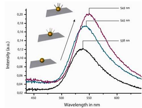
Fig.1: black – immobilized gold nanoparticle (80 nm); blue – immobilized capture oligonucleotide; purple –
hybridized target oligonucleotide; a slightly red shift after each step was detected
The project was financially supported by the German Research Foundation DFG (FR 1348/12-1)
[1] E. Hutter, and J. H. Fendler, Adv. Mater. 16, 1685 (2004).
[2] R. Möller et al., NAR 80, e91 (2000).
[3] A. Csáki et al., NAR 29, e81 (2001).
University of Bologna, Department of Biochemistry “G. Moruzzi,” Via Irnerio, 48 – Bologna 40126 Italy
e-mail: giampaolo.zuccheri@unibo.it
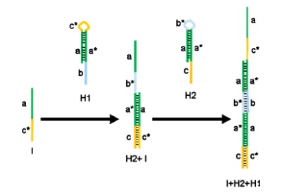
Figure 1: Scheme of the hybridization chain reaction in solution
With the goal of determining the presence of pathogens when present in very small amount, such as for
the screening of pathogens in drinking water, an analytical method of very high sensitivity must be
implemented. As often this type of determinations should be performed at the point-of-care, with simple,
automatic and inexpensive hardware, a chemical (or nanotechnological) signal-amplification step is required
prior to biosensor read-out.
The hybridization chain reaction (HCR), originally proposed by Dirks and Pierce (2004), is an isothermal,
enzyme-free process where a hybridization event triggers the polymerization of oligonucleotides into a long
albeit nicked double-stranded nucleic acid molecule. The two kinds of co-monomer oligonucleotides are
present in solution as closed hairpins, are opened and added to the growing polymer only after the initial
triggering hybridization event.
We have designed HCR oligonucleotide sets to target DNA sequences of relevance for the protection from
bioterrorism acts towards water systems. In this communication, we presents our results of the HCR
amplifications for different DNA targets of C. parvum, G. lamblia and Hepatitis E virus that have been
performed both in solution and in a microarray format, to make it more amenable of use in diagnostic or
point-of-interest assays. Our need of detecting natural occurring sequences forcedly limits our possibility of
sequence optimization, reducing it to the selection of a target sequence with low secondary structure
within a consensus sequence defined by bioinformatics tools. The design of the HCR hairpins was the
performed on the defined target sequences with the aid of NANEV (Goodman, 2005).
Our results seem to point out that there is a general sensitivity advantage in a biosensor read-out of the
presence of naturally occurring nucleic acids sequences when the hybridization chain reaction is used as a
signal-amplification step. This strategy could result of general interest for the analytical determination of
nucleic acids.
[1] Goodman, P. (2005). "NANEV: a program employing evolutionary methods for the design of nucleic acid nanostructures"
BioTechniques, 38(4): 548–550
[2] Goodman, P. (2005). "NANEV: a program employing evolutionary methods for the design of nucleic acid nanostructures"
BioTechniques, 38(4): 548–550
1 Chemical Nanoscience Laboratories, School of Chemistry, Bedson Building, Newcastle University, Newcastle upon Tyne, NE1 7RU (UK), and 2 School of Electrical, Electronic and Computing Engineering, Newcastle University, Newcastle Upon Tyne, NE1 7RU (UK)
The use of DNA as a template to control and direct metal deposition for the preparation of one-dimensional, metallic nanostructures is well-established.[1] The formation of copper nanostructures by such methods may be of particular interest due to their potential application as interconnects in future generations of nanoelectronic devices. Atomic force microscopy studies of copper nanostructures prepared using such a “DNA templating” strategy has previously been reported, whereby Cu2+ ions are first associated with “template” DNA molecules and subsequently reduced to Cu0 with ascorbic acid.[2] Here, extensive characterization of the chemical, structural, and electrical properties of copper nanostructures, prepared using this “DNA templating” method, is described.[3] Determination of the chemical composition of the nanostructured material (considered important due to the possibility for the chemical reduction of the Cu2+ ions to result in the preferential formation of Cu2O, over metallic Cu0) has been established using X-ray photoelectron spectroscopy and X-ray diffraction techniques. From these studies conclusive evidence is found that chemical reduction of the Cu2+ ions does result in the formation of the desired metallic Cu0 structures. Atomic force microscopy reveals the Cu0 structures to be 3.0 - 5.5 nm in height, and to exhibit a granular, “beads-on-a-string” morphology, see figure 1. Finally, scanned conductance microscopy has been employed as a means of probing the electrical properties of the Cu0 structures. Scanned conductance phase images of individual Cu0 nanostructures suggest that despite their metallic nature, significant levels of electrical resistance are experienced along the structures. This is thought to be a consequence of their “beads-on-a-string” morphology, and small lateral dimensions (sub-10 nm) resulting in significant electron scattering at the structure surface, as well as the presence of significant tunneling barriers at the Cu0 particle-particle junctions throughout the metal structures.
Figure 1. Tapping Mode AFM image of a Lambda-DNA-templated copper nanostructure, immobilized upon a Si/SiO2 substrate modified with a trimethylsilane self-assembled monolayer.
[1] (a) Braun, E.; Eichen, Y.; Sivan, U.; Ben-Yoseph, G. Nature, 1998, 391, 775 (b) Keren, K.; Krueger, M.; Gilad, R.; Ben-Yoseph, G.;
Sivan, U.; Braun, E. Science, 2002, 297, 72 (c) Richter, J.; Seidel, R.; Kirsch, R.; Mertig, M.; Pompe, W.; Plaschke, J.; Schackert, H.
K.; Adv. Mater., 2002, 12, 507
[2] Monson, C. F; Woolley, A. T. Nano Lett. 2003, 3, 359
[3] Watson, S. M. D.; Wright, N. G.; Horrocks, B. R.; Houlton, A. Langmuir, 2010, 26, 2068
1Friedrich-Schiller University Jena, Institute of Physical Chemistry, Helmholtzweg 4, 07745 Jena, Germany
2 Institute of Photonic Technology (IPHT) Jena, PO Box 100239, 07745 Jena, Germany
Surface enhanced Raman scattering (SERS) is an emerging tool for biological assays. It can provide
detection limits, which are at least as good as those of fluorescence and enable multiplex detection
capabilities due to the highly specific Raman fingerprint of each molecule. Due to the application of a
microfluidic system the advantages of microfluidics concerning small sample volumes as well as an
automated sample preparation and detection can be utilized.
Here we present the first results of a microfluidic system for chip-based detection using SERS. On the one
hand we used the microfluidic platform for chip-based sequence specific DNA detection using SERS. In
many cases when using microfluidics for the identification of defined DNA sequences a differentiation
between positive and negative binding events is hard to achieve since unbound labelled oligonucleotides
can not be removed by washing and therefore might be detected just as the hybridised labelled DNA
targets. This disadvantage can be circumvented by applying a chip substrate, which can be placed within a
microfluidic chamber. Due to the spatially defined alignment of different target DNA strands a sequence
specific multiplex detection is possible.
This approach can also be adapted for the detection of low molecular substances.
Acknowledgement The Funding of the Carl-Zeiss-Stiftung as well as the research project “Jenaer Biochip Initiative (JBCI within the framework “InnoProfile - Unternehmen Region” from the Federal Ministry of Education and Research (BMBF) Germany is gratefully acknowledged.