DNA Nanoarrays Printed via Dip Pen Nanolithography for High Sensitivity Bioanalysis Nabil A. Amro NanoInk, Inc, 4901 Searle Parkway, Skokie, IL 60077 Miniaturized nucleic acid in the form of nanoarrays will dramatically enhance the sensitivity, and spatial density of chip-based bio-assays. These nanoarrays will improve applications ranging from point-of-care diagnosis to genomic arrays used in basic research by enabling the development of next generation screening technologies that are faster, more sensitive, more reliable, and possibly more cost effective than those presently available in the life sciences market. Nanosized nucleic acid bioarrays can be printed using Dip Pen Nanolithography (DPN), a new direct-write spotting technology which generates sub-micron sized features of DNA or protein on solid surfaces. This printing technique offers significant advantages over current microarray printing technologies that suffer from poor spot to spot reproducibility in terms of size, shape, and oligonucleotides density, as well as reproducibility across microarray slides. Preliminary work has demonstrated that the DPN technique can be used to deposit 21mer synthetic oligonucleotides on surfaces with extremely uniform sub-100 nm to several micron scale features. The DNA nanostructures formed robust films and exhibited selectivity in binding to complementary oligonucleotides. Thus, DPN can be used to generate uniform features of synthetic DNA far smaller than those obtained with other spotting or photolithography techniques. We will describe current DPN nanoarray printing and readout technology and as well as our progress towards integrating the DPN process with MEMS and microfluidic pen loading for ultra-high throughput printing. RNA-based nanoscale integration Andrew D. Bates1, Benjamin P. Callen1, Jonathan. M. Cooper2, Rick Cosstick3, David R. S. Cumming2, Cody Geary4, Andrew Glidle2, Luc Jaeger4, John L. Pearson2, Maria Proupin-Perez3 & Cigang Xu2 1 School of Biological Sciences, University of Liverpool, UK There has of course been much focus on the development of DNA-based nanomaterials and devices, as witnessed by the array of technologies presented at this meeting. Much less attention has been paid to the potential of DNA's close analogue, RNA, in the development of designed nanoscale objects, perhaps for the obvious reasons of stability. However, RNA has some interesting potential advantages: nature provides a large array of specific tertiary interactions in highly-complex folded single-stranded RNA molecules, including cation-dependent loop-receptor and kissing-loop interactions as well as standard Watson-Crick base-pairing, which might be utilised to provide nanoscale functionality.We have adapted the tecto-RNA loop-receptor molecules developed by Luc Jaeger and co-workers to develop methods for the specific Mg2+-dependent self-assembly of gold nanoparticles. Specific RNA molecules are attached to DNA-derivatised gold nanoparticles and electrodes using standard base pairing interactions, and Mg2+-dependent RNA-RNA interactions are used to produce specific interaction between particles. Glidle, A., Jaeger, L., Pearson, J. L., Proupin-Perez, M., Xu, C., and Cumming, D. R. S. (2006) Construction and characterization of a gold nanoparticle wire assembled using Mg2+-dependent RNA-RNA interactions. Nano Lett., in press (available online - DOI: 10.1021/nl052316g). Fabrication of nanoparticle chains with rolling circle amplification Stefan Beyer, Thomas Sobey, Patrick Nickels, and Friedrich C. Simmel Department of Physics, Ludwig-Maximilians-Universität, Munich, Germany The well-established biochemical technique of rolling circle amplification allows for a simple fabrication of long single-stranded DNA molecules with a repeating sequence motif. In RCA, small circular single-stranded oligonucleotides act as templates for the polymerization of the complementary strand. A DNA polymerase with an efficient strand displacement activity - such as the polymerase from phage phi29 - can processively copy the circular template without stopping. This results in a long DNA strand with periodic sequence. We here demonstrate that this method � using DNA recognition and biotin-streptavidin binding � provides a simple procedure for DNA-directed nanoscale organization of nanoparticles. As an example, a 74 nucleotide long DNA molecule is amplified into a sequence-periodic single strand with a length up to several micrometers. Hybridization of this long periodic DNA template to the biotinylated complement of the sequence motif results in a long DNA duplex with a periodic arrangement of biotin binding sites. We show that this template can be used, for instance, to arrange streptavidin coated gold nanoparticles. Beyer, S., Nickels, P. and Simmel, F.C. (2005): Periodic DNA nanotemplates synthesized by rolling circle amplification. Nano Letters, 5, 719-722. Positioning and decoration of DNA with semiconducting conjugated polyelectrolytes Per Björk, Anna Herland, Jens Andersson, Sven Holmström, Mahiar Hamedi and Olle Inganäs Biomolecular and Organic Electronics, Department of Physics, Chemistry and Biology, Linköping University, SE-581 83 Linköping, Sweden Surface energy modification and transfer printing of DNA using soft lithography methods is used to direct DNA to specific location on surfaces via molecular combing [1]. A nanometer thin layer of low molecular species is transferred when a structured polydimethylsiloxane (PDMS) stamp is in conformal contact with a surface [2, 3]. The formed pattern is used to direct the DNA stretching. Alternatively, transfer printing of DNA using elastomeric stamps can be used to position stretched DNA. By modifying the surface properties of the PDMS stamp, the stretching properties can be altered. Stamp coating with a layer of polymethylmethacrylate (PMMA) gives a more defined stretching length compared to bare PDMS stamps.Furthermore, DNA is used as a prototype template for building nanoelectronic devices by self-assembly [4]. The electronic functions are made possible by coordinating electronically active polymer chains to DNA. The complex of DNA and the conjugated polyelectrolyte (CPE) poly(3-[(S)-5-amino-5-methoxycarboxyl-3-oxapentyl]-2,5-thiophenylenehydrochloride) (POMT) can be formed either in solution prior to stretching or after stretching of the bare DNA on a surface. Single molecular spectroscopy (SMS) in fluorescence, and microscopy, in AFM, give evidence for coordination of the short conjugated polyelectrolyte chains to the aligned DNA. SMS combined with a rotating polarizer to analyze the emitted light shows that the molecular axis of the CPE and the DNA are preferentially aligned along each other in these complexes. This is one step towards positioning of semiconducting polymers on the single molecule level, and may enable construction of electronic device function at the junction between two different polymer chains. [1] Björk P, Holmström S, Inganäs O, Soft lithographic printing of patterns of stretched DNA by surface energy modification and transfer, manuscript in progress. Biomolecular Routes for Nanoelectronics Gary Braun, R. August Estabrook, Michael Diechtierow, Falk Schmidt, Michael Lugowski, Stephanie Wilkinson, Katsuhiko Inagaki, D. K. Wood, Yan Gao, Eran Levy, Dzmitry A. Yarotski, A. V. Balatsky, Elmar Weinhold, E.L. Hu, A. N. Cleland, and Norbert O. Reich Department of Chemistry and Biochemistry, Biomolecular Science and Engineering Program,Department of Physics, and Department of Materials, University of California, Santa Barbara, California 93106-9510 The ability to position nanoparticles (NP) onto molecular scaffolds with nanometer control has potential applications for biosensors, optoelectronics, and a range of basic nanoelectronics studies. We are developing approaches for site-specific placement of NP at predetermined positions within thousands of base pairs. One approach relies on exploiting bacterial DNA methyltransferases, which normally methylate a specific base pair within a recognition sequence. In this application the protein transfers a biotin to a sequence using an artificial enzyme cofactor. We have recently shown that biotinylated gold NP can be directed to one or more of these biotin positions within 300 - 1000 nm long DNA fragments. Streptavidin binds the biotin-NP to the biotin-DNA, and constructs are routinely imaged by AFM. We have also constructed 3- and 4-way DNA junctions using streptavidin bridging, with a nanoparticle directed to the streptavidin-junction through a remaining biotin-binding site on the tetrameric protein. The combination of directed assembly at one or more DNA sites with electrostatic assembly of cationic NP onto the remaining template has been used to create hybrid metal-semiconductor, metal-magnetic, and magnetic-semiconductor NP-DNA structures. The properties of these hybrid structures are currently being explored.Proteins have previously been shown to mask regions of DNA against the binding of NP, causing a ~10 nm gap during reductive metallization into nanowires. We have used our site-specific biotinylation to position streptavidin, similarly blocking the electrostatic assembly of NP and the subsequent metallization. TEM performed on commercially available thin film windows of silica has been used to characterize the NP-NP distances and morphologies during reductive growth, while assembly conditions and surface chemistries are identical to thicker Si/SiO2 substrates used in electronic characterization. Finally, STM analysis of NP-DNA structures formed on surface-passivated doped-silicon are being characterized. The electronic coupling between NP, DNA base pairs, and the conducting substrate are being examined for both metallic and semiconductor assemblies.We have fabricated nanowires (NW) through electrostatic assembly of cationic Au NP ~3 nm onto DNA. NP seeds grow and fuse through reductive Au plating to create conductive wires. Pre-patterned electrodes by e-beam lithography are used in conjunction with thiolated DNA constructs for the positioning of DNA between electrodes, across gaps ranging from 100 to 1000 nm. Conversely, post-patterning of electrodes on top of NW structures formed from parallel arrays of stretched DNA on Si/SiO2 is being used for the analysis of large numbers of NW. A third approach uses multiple-tip conducting AFM (Multiprobe, Inc.) to characterize wires without the need for patterning electrodes. Nanowires with diameters ~40 - 100 nm synthesized from NP-seeds on DNA templates display ohmic conductivity ~1% the predicted value, and temperature dependency of resistance and annealing statistics will be described, including breakdown characteristics. Self-Assembled Supramolecular Polymers Made of DNA Parallelograms M. Brucale1, G. Zuccheri1,2,3, B. Samori1,2 1Department of Biochemistry, 2National Institute for the Physics of the Matter, 3National Interuniversity Consortium for Material Science at the University of Bologna. Via Irnerio, 48 - Bologna Italy - 40139. The self-assembly of oligodeoxynucleotides is a versatile and powerful tool towards the construction of objects in the nanoscale [1]. The strictly information-driven pairing of DNA fragments can be used to rationally design and build nanostructures with planned topologies and geometries. Taking advantage of the steadily expanding library of well-characterized DNA motifs, numerous examples of structures with a variety of shapes have appeared in the literature in the last few years, laying the foundations for a very promising DNA-mediated bottom-up approach to nanotechnology. 1. M.Brucale, G.Zuccheri, B.Samori, "Mastering the complexity of DNA Nanostructures", Trends in Biotechnology 2006 (in press) Directed DNA Metallisation: Towards The Construction Of Rationally Designed, Conductive Nano Devices Glenn A. Burley, Johannes Gierlich, Pillipp Gramlich, David M. Hammond and Thomas Carell Fakultät für Chemie und Pharmazie, Ludwig-Maximilian-Universität München, Butenandtstr. 5-13 (Haus F), D-81377 München, Germany; Our research group is interested in exploiting self-assembling macromolecules as instructional tools for the construction of rationally designed, conductive nano devices. DNA, in this respect, is a particularly outstanding architecture.1 While Watson-Crick base-pairing principles provide the basis for the templating of nucleic acid molecules into periodic arrays or predictable structures, enzymes can be used to manipulate and troubleshoot errors in the resulting constructs. DNA architectures can then be made conductive via the reduction of DNA-complexed metal salts thus offering the potential of utilising DNA constructs in molecular electronics and electrical diagnostics applications. The majority of these procedures however, produce uniformly metallised DNA architectures whereas electronic devices require programmable wiring.One strategy that provides a possible avenue towards the rational design of conductive DNA constructs is the enzymatic incorporation of modified nucleoside triphosphates (e.g. 1-4). These modified triphosphates provide functionalities that have the potential to direct the labelling process (e.g. silver reduction) via clicking of azides (5-8, in the case of triphosphates 3 and 4) to a particular gene of interest within genomic mixture of naturally occurring genes lacking these functionalities (Figure). Figure: Conceptual scheme of post-synthetic labelling of highly functionalised DNA. This presentation will describe our latest efforts towards the development of new DNA labelling strategies that enable efficient and selective fluorescent labelling, or Ag(0) deposition around aldehyde-modified DNA (2). The ability to control the metallisation process offers the possibility to exploit the arsenal of molecular biological tools in order to construct conductive DNA nano devices. 1. Seeman, N. C. Nature 2003, 421, 427-431. Atomic-force imaging of DNA on graphite and mica surfaces Benjamin Dwir*1, Dmitry Klinov1,4, Eli Kapon1, Natalia Borovok2, Tatiana Molotsky2, Alexander Kotlyar*2,3 1 Laboratory for the Physics of Nanostructures, Ecole Polytechnique Federale de Lausanne, Switzerland We characterized various DNA structures (single-, double-, triple-stranded and quadruplex-DNA) using intermittent-contact atomic-force microscopy (AFM) on two substrates: modified highly-oriented pyrolitic graphite (HOPG) and mica. We tested both natural (single-stranded phage M13 and double-stranded plasmid pSK+ DNA) and synthetic (double-stranded poly(dG)-poly(dC), triplex poly(dG)-poly(dG)-poly(dC) and G4 folded from poly(dG) DNA) molecules. Deposition on mica, a conventional substrate used in studies of bio-molecules, results in strong deformation of all above types of molecules while deposition on modified HOPG affects the morphology of DNA much less compared to mica. This is most flagrant in the case of ssDNA, where we see important agglomeration on mica (Fig. A) but not on HOPG (Fig. B). For all molecules, the measured height on HOPG was higher than on mica (Fig. C), reaching for triplex and G4 DNA values similar to those measured in solution. The lower forces exerted by the HOPG substrate result also in an increased flexibility of the molecules: measurement of the normalized end-to-end distance of 1000 bp long poly(dG)-poly(dC) and 1000 triads long triplex DNA shows a higher normalized end-to-end distance on mica (0.7�0.2) than on HOPG (0.3�0.2). This clearly indicates the higher stiffness of DNA on mica. We thus conclude that modified HOPG is a substrate that is more suitable than mica for AFM characterization of DNA morphology. Sequence-specific DNA functionalization for manipulation and detection of single DNA molecules Christophe Escude1, Benedicte Geron-Landre1, Aurelien Crut2 and Pierre Desbiolles2 1. Museum National d'Histoire Naturelle, Regulations et dynamique des genomes, Paris, France. Controlled anchoring of single DNA molecules to surfaces has promising potential applications in bioanalytics and nanotechnology. We have combined molecular biology and sequence-specific DNA binding-agents in order to construct new hybrid DNA structures. Sequence-specific DNA functionalization can be performed either at the ends of a DNA molecule or at internal positions. Using the specific hybridization properties of DNA and enzymatic ligations, we are able to construct mutibranched DNA structures in a well-controlled pattern.(1) For example, we have constructed circular DNA molecules carrying two different DNA fragments at specific sites, and also plasmid dimers.(2) 1. Geron-Landre, B., Roulon, T. and Escude, C. (2005) Stem-loop oligonucleotides as tools for labeling double-stranded DNA. The FEBS Journal, 272, 5343-.5352. Specific metal deposition onto immobilized metal nanoparticles studied on the single particle level Grit Festag, Andrea Steinbröck, Andrea Csaki, Wolfgang Fritzsche Institute of Physical High Technology (IPHT) Jena, Germany In order to realize electrical or optical activity with DNA-based constructs, metal (especially gold) nanoparticles provide a wide range of possibilities. Based on DNA-modification of particles, they can be integrated into molecular complexes made by DNA-DNA interactions. The highly specific deposition of a metal shell onto these particles represents a basic approach in DNA-based molecular construction as well as in nanoparticle-based DNA-chip technology. This process (that is based on autocatalytic reduction of metal salts at the particle surface) is studied by AFM by imaging certain regions of particle-covered surfaces after each step of metal deposition. Thereby enhancement solutions of different composition (various producers as well as home-made solutions of various compositions) are studied regarding their enhancement rate as measured by the growing height of the particles at single particle level. Other features of interest were the influence of the diameter of the seed particle on the growth process and the influence of exchange of enhancement solution. We observed for the applied conditions (nanoparticles immobilized on a substrate in a density of 0.7 (Au60) - 4 (Au15) particles / �m2 and subjected to fresh enhancement solution 2 min each) a linear growth regime. The results were complemented by TEM and single particle UV/VIS spectroscopy. Support by EU (NUCAN - NMP STREP 013775) and DFG is acknowledged. Self-assembly of carbon nanotubes by bio-directed approach Khoa Nguyen, Sebastien Lyonnais, Stephane Streiff, Laurence Goux-Capes, Marcelo Goffman , Arianna Filoramo and Jean-Philippe Bourgoin Laboratoire d'Electronique Moleculaire CEA Saclay, DSM/DRECAM/SPEC, 91191 Gif/Yvette, France Single wall carbon nanotubes (SWNTs) occupy a special place within molecular electronics. Indeed, they exist as semiconducting or metallic wires and have been used to demonstrate molecular devices like transistors, diodes or SET (single electron transistor). However, the future of this class of SWNT-based devices is to a large extent related to the development of a bottom-up self-assembly technique.Here, we will briefly present an overview of the current state of the fabrication of devices made of carbon nanotubes by using self-assembly. Despite the fact that the degree of maturity of the different nanofabrication methods is variable, we will make a critical comparison of their perspectives and an analysis of the issues to be solved before they could be integrated to the real-world applications. Then, we will discuss in details our DNA-directed approach: construction of the DNA scaffold, DNA-nanotube chemistry and DNA metallisation. This bio-directed method constitutes a genuine and complete molecular-scale bottom-up method, since it relies on recognition properties inherent to biological entities and can be employed without using any standard nanolithography technique. This work is partially supported by the NUCAN - NMP STREP 013775 project DNA-based approaches for micro-nano integration Wolfgang Fritzsche, Andrea Csaki, Andreas Wolff, Robert Kretschmer, Thomas Schüler Institute of Physical High Technology (IPHT) Jena, Germany DNA is probably the most promising molecule for the construction of a wide variety of materials and devices utilizing molecular units. Integration into todays microsystems technology provide access to these interesting but usually solution-born (and thereby difficult to controll) constructs. A variety of techniques to realize this combination has been developed. Of special interest are techniques that are open for massive parallelization in order to provide today sufficient numbers of experimental setups, but also to allow for a potential scale-up on the way to future applications. We present here an overview about technical developments in this direction addressing the integration problem. Support by EU (NUCAN - NMP STREP 013775) is acknowledged. Covalent Hemin-DNA Adducts for Generating a Novel Class of Artificial Heme Enzymes Ljiljana Fruk, Joachim Müller, Christof M. Niemeyer Univ. Dortmund, FB Chemie, Biologisch Chemische Mikrostrukturtechnik, Otto Hahn Str. 6, 44221 Dortmund Today, the scientific and technological interest is moving towards the production of enzyme arrays. Thus, there is a great interest in developing technologies to precisely organize and integrate enzymes into highly ordered micro- and nanostructured assemblies.1 One approach to this goal is the DNA directed immobilization (DDI) which makes use of the specificity of DNA base pairing to anchor proteins to surfaces of planar substrates or nanoparticles.2 The DDI method offers many advantages over conventional immobilization methods, in particular, mild reaction conditions, high efficiency of immobilization and site selectivity of attachment. 1. C. M. Niemeyer, C. A. Mirkin, Nanobiotechnology: Concepts, Methods and applications, Wiley-VCH, Weinheim, 2004. Parallel Assisted Self-Assembly of Multilayer DNA and Protein Nanoparticle Structures Using a CMOS Electronic Array Michael J. Heller, Dietrich A. Dehlinger, Benjamin D. Sullivan and Sadik Esener University of California San Diego, Department of Bioengineering and Department of Electrical and Computer Engineering, La Jolla, CA 92093-0412 USA A CMOS electronic microarray device was used to carry out the assembly of functionalized nanoparticles into multilayer structures. Electronic microarrays produce reconfigurable DC electric fields that allow DNA, proteins and other charged molecules to be rapidly transported from the bulk solution and addressed to any activated site on the array surface. Such a device was now used to carry out the highly parallel assisted self-assembly of DNA, biotin and streptavidin derivatized nanoparticles into multi-layer structures. Nanoparticle addressing was carried out in 15 seconds or less, and multilayer structures with as many as forty alternating layers could be completed in less than one hour. The final 3D nanostructures were verified by scanning electron microscopy. Monitoring dielectrophoretic collection of DNA by electrical impedance spectroscopy R. Hölzel and F. F. Bier Fraunhofer Institute for Biomedical Engineering, Molecular Bioanalytics and Bioelectronics D-14558 Nuthetal / Potsdam, Germany Spatial manipulation and positioning of macromolecules like proteins and DNA by electrical means has gained increasing interest in recent years. Whilst electrophoretic lateral movement is performed in DC fields, inhomogeneous AC fields can be used not only for the attraction of molecules by dielectrophoresis, but also for stretching and parallel alignment of elongated molecules. Although the method is rather simple, not much is known about the influence of experimental parameters like medium composition and field properties. The molecules' response usually is monitored by fluorescence microscopy or subsequent atomic force microscopy. To allow for an alternative approach that makes feasible the simultaneous monitoring of the molecules' response without chemical modifications like fluorescence labelling we are applying electrical impedance spectroscopy in parallel to dielectrophoretic manipulation. The alternating current flowing through the medium between the electrodes is influenced by the macromolecules in the current path and hence is a measure of their local concentration. Here we present several experimental realisations of such a setup, mainly aimed at decoupling of the sensing field from the dielectrophoretic field and at optimising the system's sensitivity. Experimental results are compared to fluorescence microscopy. Possible applications are the development of protocols for electric field supported assembly of nanostructures and of biomolecular sensors for the detection of few or even single molecules. Integrated Bioanalytical Microdevice Utilizing Nanoparticles I-Ming Hsing Department of Chemical EngineeringProgram Director, Bioengineering Program, School of EngineeringHong Kong University of Science and Technology, Hong Kong SAR, China This talk will highlight the recent development of the bioanalytical microsystem research in my laboratory. In particular, silicon/glass based microdevices utilizing magnetic nano/micro particles for on-chip DNA separation, amplification and electrochemistry-based sequence-specific detection will be delineated. A novel technique based on the electric field fractionation principle for the separation of nanoparticles and DNA molecules in a microdevice environment will also be presented. Strategies for the on-chip implementation of an electrochemistry-based real-time polymerase chain reaction (PCR) technique for nucleic acid quantification and sequence-specific recognition will be discussed. The integrated biomicrodevice developed herein will be very useful for point-of-care diagnostics and decentralized environmental monitoring. High-resolution atomic-force imaging of DNA Dmitry Klinov1,4, Benjamin Dwir*1, Eli Kapon1, Natalia Borovok2, Tatiana Molotsky2, Alexander Kotlyar*2,3 1Laboratory for the Physics of Nanostructures, Ecole Polytechnique Federale de Lausanne, CH-1015 Lausanne Switzerland, 2Department of Biochemistry, George S. Wise Faculty of Life Sciences, and 3Nanotechnology Center, Tel Aviv University, Ramat Aviv, 69978 Israel, 4Shemyakin-Ovchinnikov Institute of Bioorganic Chemistry, Russian Academy of Sciences, 117871, Moscow, Russia. We have developed a novel high-resolution atomic force microscopy (AFM) imaging technique enabling detailed characterization of DNA morphology. We have utilized low-amplitude non-contact AFM with high-resolution [1] (tip radius 1-2 nm, Fig. A) AFM probes to image DNA adsorbed on chemically modified highly oriented pyrolitic graphite (HOPG) substrates. We have previously shown [2] that different types of DNA molecules: single-stranded, double-stranded, triplex and quadruplex DNA show a larger measured height and increased flexibility (measured by end-to-end distance) when deposited on HOPG rather than on mica(the most commonly used substrate for AFM investigation), resulting from reduced surface interaction forces on HOPG. Using the high-resolution probes and reduced-force intermittent-contact AFM imaging we could achieve high-resolution images of the triplex DNA, showing single-, double- and triple-stranded fragments in the molecules (Fig. B). Detailed height and width analysis of the AFM images (Fig. C) shows the almost linear height and width dependence on the number of strands (Fig. D), where the difference corresponds well to the diameter of the AFM probe (3 nm). By this high-resolution imaging we could follow the reaction of the G-strand extension in poly(dG)-poly(dC) by Klenow exo-fragment of DNA Polymerase I, a reaction that leads to the formation of a poly(dG)-poly(dG)-poly(dC) triplex [3] (Fig. E). High-resolution image of poly(dG)-poly(dC) double-stranded DNA is shown in Figure F. The dsDNA molecules contain fragments ('loops'), where the two strands are decoupled and can be seen as two single strands not associated with one another. The novel high-resolution method of molecular visualization described herein makes possible to investigate the molecular mechanisms of DNA replication and transcription, as well as other processes associated with changes in the morphology of DNA and other biomolecules. 1. D. Klinov and S. Magonov, Applied physics letters 84, 2697-2699 (2004). Enzymatic synthesis of novel triplex DNA nanostructures Alexander Kotlyar1,2, Natalia Borovok1, Tatiana Molotsky1 Dmitry Klinov3, Benjamin Dwir4, Eli Kapon4. 1Department of Biochemistry, George S. Wise Faculty of Life Sciences, Tel Aviv University, Ramat Aviv, 69978 Israel, 2Nanotechnology Center, Tel Aviv University, Ramat Aviv, 69978 Israel, 3Shemyakin-Ovchinnikov Institute of Bioorganic Chemistry, Russian Academy of Sciences, 117871, Moscow, Russia, 4Laboratory for the Physics of Nanostructures, Ecole Polytechnique Federale de Lausanne, CH-1015 Lausanne Switzerland. We developed the synthesis of novel long (thousand triads) triplex DNA nanostuctures. We used 1000 base pair poly(dG)-poly(dC) produced as described by us earlier [1] as a starting material for the synthesis. We have shown that extension of the G-strand in poly(dG)-poly(dC) by Klenow exo� fragment of DNA Polymerase I in the presence of dGTP leads to the formation of a complete poly(dG)-poly(dG)-poly(dC) triplex structure [2] composed of 1000 triads, each stabilized by Hoogsteen hydrogen bonds between the two G- and the one C-bases. The enzyme-catalyzed synthesis of poly(dG)-poly(dG)-poly(dC) proceeds through sequential elongation of the poly(dG) strand of the double stranded poly(dG)-poly(dC) molecule, and folding of polyG de novo back on the poly(dG)-poly(dC) [2]. The synthesis was followed by direct imaging of molecular morphology of the products using a novel high-resolution atomic force microscopy (AFM) imaging technique. A series of 'snapshot' images of the molecules, which reflects the dynamics of the synthesis, is demonstrated in the figure below. The length of the triplex fragment (seen as bright fragment in the figure) increases with the synthesis time together with the reduction of the length of the remaining double stranded fragment (seen as a narrower and darker fragment in the figure). The different brightness of fragments along the synthesized molecule is due to a difference in height of the triplex and the double stranded DNA. The heights of the poly(dG)-poly(dG)-poly(dC) triplex and of the poly(dG)-poly(dC) duplex measured on modified graphite are 2�0.1 and 1.0 �0.1 nm, correspondingly. This two-fold increase in the apparent height of the triplex with respect to that of the duplex reflects the higher stiffness of the former molecules and their resistance to the surface adhesion forces and to the pressure of the AFM tip.High resistance of the synthesized triplexes to mechanical forces, a large surface area of the GGC triad, and high content of G-nucleotides in the molecules all together suggest that poly(dG)-poly(dG)-poly(dC) nanostructures might have improved conductive properties with respect to the double-stranded DNA. 1. A.Kotlyar, N.Borovok, T.Molotsky, L. Fadeev and M. Gozin, Nucleic Acid Res. 33, 525 (2005). Nanocrystals Coated with an Amphiphilic Polymer Shell: A route to water soluble nanocrystals of different Shapes Pei-yun A. Liab, Cheng-an J. Linab, Marco Zanellaa, Ralph A. Sperlinga, Jimmy K. Lib, Teresa Pellegrinoc, Liberato Mannac, Walter H. Changb, Wolfgang J. Paraka a Center for NanoScience and Ludwig-Maximilians-Universitat Munich, Germany High-quality colloidal nanocrystals of various materials can be synthesized in hot organic solvents. This route typically yields roughly spherical nanoparticles with a diameter of a few nanometers. From our previous experience[(1-4)], rod- & tetrapod-shaped nanocrystals can be also grown by similar organometalic chemistry. In order to use hydrophobic nanoparticles for further biological applications, they first have to be transferred into aqueous solution. Here we demonstrated a general strategy which allows for transferring hydrophobically capped nanocrystals with different shape from organic to aqueous solution by wrapping an amphiphilic polymer around the particles. poly(maleic anhydride alt-1-tetradecene) is a good candidate of amphiphilic polymer which can mediate the hydrophobic nanomaterials to become water soluble. The amphiphilic polymer is wrapped around the nanoparticle, whose hydrophobic chains intercalate the hydrophobic stabilizing molecules bound to the particle, whereas the hydrophilic parts of the polymer endow water-solubility. For further stabilization, the cross-linker is necessary from our experience. 1. Manna L, Scher EC, Alivisatos AP. Synthesis of Soluble and Processable Rod-, Arrow-, Teardrop-, and Tetrapod-Shaped CdSe Nanocrystals. Journal of the American Chemical Society 2000;122(51):12700-12706. Synthesis of monofunctionalized nanoparticles by using poly(ethylene glycol) Cheng-an J. Linab, Ralph A. Sperlinga, Jimmy K. Lib, Pei-yun A. Liab, Teresa Pellegrinoc, Liberato Mannac, Walter H. Changb, Wolfgang J. Paraka a Center for NanoScience and Ludwig-Maximilians-Universitat Munich, Germany Nanoparticles with defined functional group are the basic building block of design of complex nanodevices. Here we described a general concept of monofunctionalized nanoparticles which facilitates the modification of different nanomaterials with an exactly known number of functional groups. From our previous results(1, 2), the amphiphilic polymer coating is a good technique to transfer hydrophobic nanomaterials to water soluble such as CoPt3, Au, CdSe/ZnS, and Fe2O3. We can easily modify different nanomaterials into the same surface chemistry, i.e. the carboxyl group (-COOH), which could further covalently coupled with other ligand molecules containing primary amine by means of EDC chemistry. Nanoparticles modified with poly(ethylene glycol) (PEG) show an increased salt stability, even in physiological cell media, caused by the steric repulsion of the polymer chains with associated H2O molecules. If the carboxylated nanocrystals coupled with PEG molecules of suitable chain length (Mw >5,000 ), conjugates of nanoparticles with one, two, and three PEG molecules per nanoparticle could be separated by running through the gel electrophoresis. Molecules with additional functionalities could be conjugated to the free ends of the bifunctional PEG molecules. In this way the PEG molecules act as convenient spacers that allow for the sorting of nanoparticles with a discrete number of functional groups. Stretching and positioning of individual DNA molecules on electrodes by the electrohydrodynamic force Hung-Yi Lin1, Li-Chu Tsai2, Pei-Yin Chi3 and Chii-Dong Chen3 1 Department of Natural Science Education, National University of Tainan, Taiwan, ROC Stretching of individual DNA molecules provides a useful system for study molecular nanotechnology. In this report, we propose and demonstrate a method for the positioning of unmodified extended DNA molecules. A local microscopic cyclic flow is created by a non-uniform AC field and utilized to carry the lambda-DNA over the electrode surface repeatedly. With a proper choice of the solution pH, the moving DNA can be anchored and stretched on a gold surface (Figure a,b) or between gold electrodes[1]. The electrical-field amplitude and frequency responses of DNA motion are studied. The method can be applied to position the DNA with accuracy on a microscopic scale while requiring no modification of the DNA for terminal binding. With a diluted DNA solution, the number of DNA across the electrodes is controllable and the positioning of a single extended DNA across electrodes is achievable. The position accuracy is limited by the visibility of the molecules. 1. H. Lin, L. Tsai, P. Chi and C. Chen, Nanotechnology 16 (2005), 2738-2742. DNA templates and carbon nanotubes non-covalent linkage S. Lyonnais, L. Goux-Capes, C. Escue*, S. Streiff, A. Filoramo and J.-Ph. Bourgoin Laboratoire d'Electronique Moleculaire CEA Saclay, DSM/DRECAM/SPEC, Gif/Yvette, France. The properties that make DNA so successful in acting as a genetic material also make it a convenient and logical molecule to use for constructing new materials on the nanometer scale. Particularly, the exceptional molecular recognition properties of DNA through specific base-pairing make it a promising candidate for the assembly of future nano-electronics circuits and site-controlled implementations of nano-components. Indeed, DNA is currently engineered to both create scaffolds and self-assemble nanomaterials [1]. Within this context, biological recognition has been imparted to single-wall carbon nanotubes (SWNT), which are actually prime candidates for novel nanoelectronics applications [2]. Indeed, SWNT self-assembly, mediated by DNA into functional devices has been already successfully demonstrated [3]. This work is partially supported by the NUCAN - NMP STREP 013775 project [1] Seeman N. C., Nature 2003, 421, 33; Seeman N. C., Nanotechnology, 1991,2, 149; Mirkin C. A., Inorg. Chem. 2000, 39, 2258. A New Triple Crossover Triangle (TXT) Motif for Higher Order DNA Architecture Bryan Wei and Yongli Mi* Department of Chemical Engineering, Hong Kong University of Science and Technology, Clear Water Bay, Kowloon, Hong Kong, * keymix@ust.hk A new triple crossover triangle (TXT) motif was conceived based on the DNAtriple crossover (TX) motif. The new motif is rigid and triangular prism shaped, out ofwhich 1-D, 2-D, and 3-D DNA structures can be assembled. The 1-D TXT array wasself-assembled and was observed by the TEM with the negative staining by uranylacetate. The architectural schemes for 2-D and 3-D structures are presented. There are atleast three reasons why we introduce the TXT motif to DNA self-assembly research.Firstly, because the motif is in a triangular prism shape, it is almost certainly more rigidthan the existing planar DNA motifs. Secondly, in the 2-D array, the TXT motif can beself assembled following the algorithm of the DX array, and, in addition, leaving an extradiscontinuous DNA double helices layer above, which is open for further modificationswithout affecting the desired array. Because of the extra layer of the DNA double helices,the height of the array is doubled. Thirdly, most importantly, TXT motif can be used forbuilding 3-D arrays. With appropriate sticky ends matching strategies, TXT motifs,which are, by themselves, 3-D, can be packed to form 3-D arrays. A computer program,Uniquimer, is developed for the design of DNA self-assembly. Research Funding: RGC 602405 Controlled DNA Synthesis and Construction Kalim Mir, Giuseppe Scozzafava, Hong Qi, Oleg Salata, Alex Krieg and Heidi Dvinge The Wellcome Trust Centre for Human Genetics, Roosevelt Drive, Oxford OX3 7BN, UK We are exploring methods to exert control over molecular construction. This work involves developing means for controlling template-directed DNA synthesis with nucleotide or oligonucleotide building blocks, using reversible termination and studying the process on microarrays and at the single molecule level. We are also interested in studying the interactions of oligonucleotides with structured nucleic acids and developing means for controlling molecular interactions using allosteric and cooperative mechanisms. In addition, our work involves integrating bottom-up self assembly from the solution-phase with top-down manufacture of oligonucleotide array chips. We are applying aspects of the work to the development of novel DNA sequencing technology. Kinetic study of semisynthetic DNA-enzyme conjugates Joachim Müller, Ljiljana Fruk and Christof M. Niemeyer Univ. Dortmund, FB Chemie, Biologisch Chemische Mikrostrukturtechnik, Otto Hahn Str. 6, 44221 Dortmund We have developed a novel approach to produce well defined and functional DNA-enzyme conjugates which can be used for arrangement of enzymes on both nano- and microscale. Our approach is based on reconstitution of apoenzymes with DNA modified cofactors.[1] Detailed kinetic studies of DNA-enzyme activity were performed in solution and with conjugates immobilized on solid surfaces.[2] The results showed a large increase of peroxidase activity for DNA-myoglobin conjugates, while the reactivity of horseradish peroxidase was decreased. All conjugates were successfully immobilized using DNA-directed immobilization (DDI) and remained active.The programmable binding properties enabled by DNA hybridization make such semisynthetic enzyme useful for a broad range of applications, particularly in biocatalysis, electrochemical sensing and as building blocks for biomaterials. [1] L. Fruk, C.M. Niemeyer, Angew. Chem. Int. Ed. 2005, 44, 2603-2606. DNA-Templated Metallic Nanowires. K. Nguyen, L. Goux-Capes, M. Goffman, A. Filoramo, J.-Ph. Bourgoin Laboratoire d'Electronique Moleculaire CEA Saclay, DSM/DRECAM/SPEC, 91191 Gif/Yvette, France Nanotechnology aims to produce and manipulate well-defined structures at the nanoscale level with high accuracy. However, nowadays is well admitted that conventional technologies based on the "top-down� approach are foreseen to experiment difficulties due to various physical effects that do not scale properly, and most important, related to the cost issues of the fabrication processes at the nanoscale dimension. This is a prompt for the study of new methodologies based on bottom-up approaches. In this framework, DNA molecule is of particular interest since, thanks to its unique intra- and intermolecular recognition properties, it has been already used to build-up nanostructures (1,2) or scaffolds for nanoparticles assembly (3) and it can be envisioned for the assembly of devices. Our ambition is also to utilize DNA not only as a positioning scaffold for nanodevices but also as a conducting element. In order to ensure good DNA transport properties when this molecule is deposited on dry substrate like in nanodevice configuration we found that the best way is to perform its metallization. Here we report a method based on Electroless Plating of platinum/palladium ions which bind to DNA bases and serve as catalytic spots for further metal growth (4). The key point is to develop a technique to metallize DNA only after its deposition onto the substrate. This is indeed essential since DNA loses its recognition properties after the metallization step. Therefore the process should be performed on a surface which can be directly used for molecular electronics purposes. Furthermore we have fabricated thin and conductive nanowires, limiting parasitic surface metallization by appropriate substrate treatments. Fig. 1. AFM images of combed and metallized lambda-DNA This work is partially supported by the NUCAN - NMP STREP 013775 project [1] N. C. Seeman, Nature 421 (2003), 33-37 Ferrocenyl-Modified DNA: Synthesis and characterization of 12-mer oligonucleotides in solution and after integration with semiconductor electrodes Andrew R. Pike University of Newcastle upon Tyne The ferrocenyl-nucleoside, 5-ethynylferrocenyl-2'-deoxycytidine was prepared by the Pd-catalyzed Sonogashira coupling reaction between ethynylferrocene and 5-iodo 2'-deoxycytidine. It was then incorporated into oligonucleotides through automated solid-phase synthesis at both commercially available silica supports and also at modified single-crystal silicon electrodes. Electrical transport, polarizability and spectroscopy measurements through DNA molecules and derivatives using conductive AFM and STM Hezy Cohen1, Claude Nogues,1,2 Daniela Ullien,1 Tomer Sapir,1Errez Shapir,1 Natalia Borovoka,3 Tatiana Mototskya,3 Ron Naaman,2 Alexander Kotlyar,3 and Danny Porath1 1- The Hebrew University of Jerusalem, Israel 2- The Weizmann Institute, Rehovot, Israel, 3-Tel Aviv University, Israel DNA is considered as one of the attractive candidates for molecular electronics due to the high density of its components, its accurate synthesis and its double-strand recognition properties that suggest self-assembly. DNA was studied in many ways including: electrical transport, atomic force microscopy (AFM) and scanning tunneling microscopy (STM). It seems that the results of the various measurements of charge transport in DNA are not consistent. A deeper look into the experiments can offer a general understanding of the reports and ways to optimize the conductivity in DNA. Rolling circle amplification for spatially directed synthesis of a solid phase anchored ssDNA molecule Edda Reißa, Ralph Hölzel,a Markus von Nickisch-Rosenegk,a Frank F. Bier,a,b a Fraunhofer Institute for Biomedical Engineering, Department of Molecular Bioanalytics & Bioelectronics, D-14558 Nuthetal, Germany b University of Potsdam, Institute of Biochemistry and Biology, Potsdam, Germany DNA self-assembly is a promising tool for the development of ordered nano-scale structures. If single-stranded DNA is used as a basic building block, it can be easily addressed by complementary base-pairing. However, the problem of constructing nano-structures in a defined manner with a high spatial resolution has not been solved up to now. Today, stretching of DNA usually is done by combing or the application of an electric field. DNA adsorption on inorganic surfaces and nanostructure growth Bruno Samori,1,2 Giampaolo Zuccheri,1,2,3 Marco Brucale,1 Pasquale De Santis,4 1 Department of Biochemistry, 2 National Institute for the Physics of the Matter , 3 National Interuniversity Consortium for Material Science at the University of Bologna. Via Irnerio, 48 � Bologna Italy - 40139. 4 Department of Chemistry, University of Rome La Sapienza. Italy. The preparation of DNA-based nanostructures is usually accomplished in solution, by the controlled-temperature assembly of a number of oligonucleotides into complex, often multi-modular structures. Several techniques are then used to lay the nanostructures on solid surfaces, either to make them amenable to further studies with surface techniques (such as the atomic force microscope) or to integrate them on microfabricated devices. The adsorption of nucleic acids on inorganic surfaces can take place with orientational preference as a function of the DNA base sequence. Evidence was obtained of the capability of the mica surface of recognising the two faces of a strongly curved DNA fragment.[1] The differential free energy involved in that recognition mechanism was estimated, and the modulation, by the same recognition process, of the conformational space accessible to a DNA molecule upon its deposition on mica was evidenced. On the basis of these data a tentative model based on sequence-dependent unbalances of the charge distribution along the chain is proposed. This model suggests that the crystal surface can recognise such unbalances of charge, and that the recognition process does not necessarily require curved tracts: it could act also in straights DNAs.[2]A fine control of surface adsorption properties could also prove beneficial for the control and tailoring of DNA-based nanostructure growth, as this can be accomplished directly on surfaces. We have evidence that growing DNA nanostructures based on the stable Holliday junction could take place through only some of the possible pathways when performed on the surface, if compared to solution growth. We collected experimental data on a system based on the DNA parallelogram motif introduced by Prof. Seeman [3] where the assembly could be made more efficient to the point that kinetically-trapped unwanted structures could be avoided by forcing the growth to take place while all the components are adsorbed on a surface. As a fringe benefit, the reduction of dimensionality inherent in the surface adsorption enables the assembly to take place at strongly reduced oligonucleotide concentrations if compared to solution assembly. [1] Sampaolese, B., Bergia, A., Scipioni, A., Zuccheri, G., Savino, M., Samori, B., and De Santis, P. Recognition of the DNA sequence by an inorganic crystal surface. Proc Natl Acad Sci U S A, 2002. 99(21): p. 13566-70. Fabrication of microelectrodes by self-organization of metal enhancement seeds Thomas Schüler, Robert Kretschmer, Robert Möller, Wolfgang Fritzsche Institute of Physical High Technology (IPHT) Jena, Germany The rise of DNA-chip technology pushed the development of devices for positioning of small droplets of DNA-containing solutions on chip surfaces. This approach was combined with recent advances in enzymatic metal deposition techniques in order to realize microelectrode structures by spotting of precursor molecules prior to metal enhancement. Thereby various combinations of complementary DNA-DNA-interactions, molecular coupling based on biotin-(strept)avidin and highly specific metal deposition techniques were utilized in order to fabricate conductive lines connecting prestructured photolithographic microelectrodes on a chip. Microscopical as well as electrical characterization demonstrated the proof-of-concept but also pointed to shortcomings, especially regarding overall feature size and problems in homogenity of the structures. Support by EU-FP6 (NUCAN - NMP STREP 013775) is acknowledged. Using Structural DNA Nanotechnology To Organize Matter Nadrian C. Seeman Department of Chemistry, New York University, New York, NY 10003, USA Structural DNA nanotechnology uses branching to produce unusual motifs that can be self-assembled into objects, lattices and devices. The self-assembly process is directed by programmable cohesive interactions between the ends of the helices, typically using single-stranded overhangs called 'sticky ends'. The strength of sticky-ended cohesion is that it produces predictable adhesion combined with known structure. Initial constructions included stick-polyhedra, knots and Borromean rings. These were followed by the self-assembly of two-dimensional arrays built from simple motifs, such as double (DX) and triple (TX) crossover motifs. Recent array components include planar and skewed triangular motifs whose edges are DX molecules. The former leads to honey comb-like arrangements, as shown on the left below. We combine DNA motifs to produce specific structures by using sticky-ended cohesion (below, left). Transistor in a test tube and antibodies to semiconductors Uri Sivan Department of Physics and the Russell Berrie Nanotechnology Institute, Technion-Israel Institute of Technology, Haifa, Israel In recent years we have progressed significantly in harnessing molecular biology to the self-assembly of simple nanoelectronic devices. Utilizing DNA templates and recombinant proteins we demonstrated sequence specific molecular lithography and self-assembly of a functional transistor made of non-biological ingredients. Self-assembly of more elaborate structures requires, though, additional tools and in particular establishment of a functional interface between the resulting electronic signals and the bio-assembly process. In the context of hierarchical assembly of logic gates made of our self-assembled transistors, such an interface is needed in order to filter out faulty devices before their integration into gates. In the talk I will present our ongoing efforts to establish such an interface based on the selection of antibodies that recognize electrostatic potential landscapes presented to them by the electronic system. Such an interface may conversely serve to gain electronic control over bio-reactions. Manipulation of Biological Surfaces at the Nanoscale: Prerequisites, Developments, Examples Hartmut Stadler Veeco Instruments GmbH, Dynamostr. 19, D-68165 Mannheim, Germany Scanning probe microscopy (SPM) offers nanometer resolution in three dimensions and can be operated under physiologically relevant conditions (liquid flow, temperature control). Therefore SPM is a powerful tool in nanotechnology to study biological processes on surfaces in-situ and in realtime. Besides the investigation of surface morphology or the direct measurement of interaction forces, nanometer scale positioning accuracy and tip movement control allows for precise manipulation of species at the interface. Selective Functionalization of Carbon Nanotubes by Biological Compounds S. Streiff, S. Lyonnais, L. Goux-Capes, A. Filoramo, and J.-Ph. Bourgoin Laboratoire d'Electronique Moleculaire CEA Saclay, DSM/DRECAM/SPEC, 91191 Gif/Yvette, France Carbon nanotubes (CNTs) have recently received a very large attention due to their striking mechanical and electrical properties. In particular, their quasi one-dimensional structure makes them prime candidates for nanoelectronics applications. In the framework of alternative nanofabrication technologies, combining DNA-directed assembly with SWNTs electronic properties seems a solution of choice to develop a versatile self-assembling technique for the fabrication of nanotube devices and circuits. AFM image of SWNT functionalized at the ends by DNA strands This work is partially supported by the NUCAN � NMP STREP 013775 project [1] Ph. Avouris, Review article in MRS Bulletin 2004, 29, 403-410. Dielectrophoresis of nanoscale dsDNA using metallic and CNT-electrodes: Humidity effects on dsDNA's electrical conductivity J.J. Toppari, S. Tuukkanen, A. Kuzyk, V.P. Hytönen*, T. Ihalainen* and P. Törmä Nanoscience Center, Department of Physics and *Department of Biological and Environmental Science, P.O. Box 35 (YN), FIN-40014 University of Jyväskylä, Finland Dielectrophoresis (DEP) has been widely used as an active manipulation method for micron-scale objects, especially for biological ones due to its delicate nature. The DEP-force is determined by the magnitude of electric field gradient and particle polarisability. Thus, for nanoscale objects higher field gradients are needed to overcome the Brownian motion and realize the trapping. This further requires smaller electrodes. We have developed AC-DEP technique to trap, straighten and attach nanoscale thiol-modified double-stranded (ds)DNA molecules between nanoelectrodes [1]. The technique has a reasonably high yield allowing repeatable and reliable electrical conductivity measurements of single or a few molecules. [1] S. Tuukkanen, A. Kuzyk, J.J. Toppari, V.P. Hyt�nen, T. Ihalainen and P. Törmä, APL 87, 183102 (2005). Auto-orientation of G-wire DNA Networks James Vesenkaa,c, David Bagga, Andreas Wolffb, Anett Reichertb, Robert Moellerb, and Wolfgang Fritzscheb a Chemistry/Physics Dept., Univ. of New England, Biddeford, ME 04005 USA Scanning probe microscopy was used to examine small (~50 nm) segments of quadruplex DNA polymers, a.k.a. �G-wires�, after adsorption onto mica (Fig. a). The angles the G-wires made with the fast scan direction were measured (Fig. b). The angle-frequency information was compared with the underlying lattice structure of the mica substrate (Fig. c). The G-wires appear to have a preferential orientation at 60� intervals after thorough rinsing and slow drying upon the surface of freshly cleaved mica. This orientation could be quantitatively characterized by a correlation coefficient. A model is proposed to explain this auto-orientation affect due to alignment of the G-wires� phosphate backbone and the underlying mica lattice. Pairs of adjacent, parallel phosphate groups of the G-wires (0.95 nm apart) appear to align with the next nearest neighbor potassium vacancy sites of mica (0.90 nm apart). This behavior is not observed in solution. The potential for using the auto-orientation phenomena in the development of high-density biomolecular nano-electronic devices was also explored. Adsorption and Surface Dynamics of short DNA and LNA oligonucleotides on Single-Crystal Au(111) Electrode Hainer Wackerbarth Technical University of Denmark, Department of Chemistry, Lyngby Oligonucleotide-based molecules assembled in adlayers on solid/aqueous solution interfaces have become the basis for novel biotechnology known under appellations such as DNA-chips and DNA-based biosensors. The highly specific self-assembling properties of DNA makes it attractive as a component for electronic elements in nanoscale and single-molecule devices. A novel, broad and versatile class of nucleic acids, the locked nucleic acids, or LNAs has come to offer equally exciting perspectives. The difference between the LNAs and the DNA-based molecules is that the furanose rings are locked into a C3'-endo conformation by insertion of an oxymethylene group between the C2' and C4' atoms. This gives much stronger hybridization than for normal DNA-based molecules even for short oligonucleotides. [1] H.Wackerbarth, M. Grubb. J. Zhang, A.G. Hansen, and J. Ulstrup J. Solid St. Electrochem. 8 (2004) 474. Charge pattern formation at silicon surfaces for defined biomolecule adsorption A. Wolff1, W. Fritzsche1, M. Reiche2, M. Seibt3, X. Yu4, M. Kittler4 1Institute of Physical High Technology (IPHT) Jena, Germany; 2MPI f. Mikrostrukturphysik, Weinberg 2, Halle, Germany; 3IV. Physikal. Inst., Georg-August-Univ., Friedrich-Hund-Platz 1, Göttingen, Germany; 4IHP, Im Technologiepark 25, Frankfurt (Oder), Germany Defined placement of biomolecules at Si surfaces is a precondition for a successful combination of Si electronics with biological applications. We aim to realize this by Coulomb interaction of biomolecules with dislocations in Si. These dislocations will form negatively (positively) charged lines in n-type (p-type) Si and will be surrounded with a space charge region (Read cylinder) being connected with an electrostatic barrier. This barrier forms an electric field reaching up to a few kV/cm. A regular dislocation network can be formed by wafer direct bonding at the interface between the bonded wafers in case of a misorientation, whereas ideal bonding of two wafers with identical orientation would not form a dislocation network. The adjustment of the misorientation allows the variation of the distance between the dislocations in range from about 10 nm to a few microns. This is an appropriate range for applications in nanobiotechnology dealing with protein or DNA molecules with sizes in the nanometer and lower micrometer range. We have already achieved a minimum distance between the dislocations of about 20 nm, according to transmission electron microscopy data. Also, the existence of a distinct electrostatic barrier/field at the interface containing the dislocation network was demonstrated by the EBIC technique. Thus, we demonstrated the existence of an electric field at dislocations generated by wafer bonding inside the Si material, which is essential for the outlined project. Because of the relatively short range of this field (smaller than one micron) the dislocation network has to be placed close to the Si surface. We placed the dislocation network in an interface running in very close distance of only 150 nm parallel to the Si surface by corresponding preparation, including the smart cut� (smaller distances can be achieved).In summary, we demonstrated that regular dislocation networks formed by bonding close to the Si surface might be used for self-organized placing of biomolecules. Experiments are currently underway to test whether biomolecules decorate the pattern of the dislocation lines. This project is supported by the VolkswagenStiftung.
2 Department of Electronics and Electrical Engineering, University of Glasgow, UK
3 Department of Chemistry, University of Liverpool, UK
4 Department of Chemistry and Biochemistry, UC Santa Barbara, USA
[2] Glasmästar K, Gold J, Andersson AS, Sutherland DS, Kasemo B, 2003 Langmuir 19(13) 5475-5483.
[3] Wang X, Tvingstedt K, Inganäs O, 2005 Nanotechnology 16(4) 437-443.
[4] Björk P, Herland A, Scheblykin IG, Ingan�s O, 2005 Nano Lett 5(10) 1948-1953.
University of Heidelberg, Germany; Institute of Organic Chemistry
RWTH Aachen University, Germany
Condensed Matter and Thermal Physics Group, Los Alamos National Laboratory, Los Alamos, New Mexico
Department of Applied Physics, Hokkaido University, Sapporo 060-8628, Japan
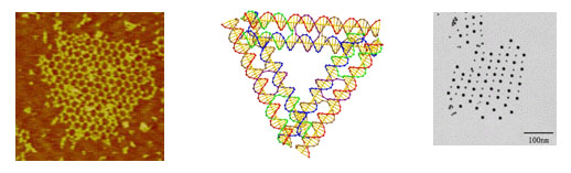
In this poster, we describe the design and synthesis of a class of DNA supramolecular constructs resulting from the polymerization of a self-complementary module in different controlled conditions. This module is a DNA parallelogram [2] constituted by six oligonucleotides with lengths varying from 42 to 59 bases, that upon thermal annealing self-assemble into the desired shape. The vertexes of the parallelogram are Holliday junctions, and its edges are 21 bp-long double helices. To our knowledge, this makes the parallelogram we are describing the smallest reported to date. Each parallelogram can bind to exactly two other parallelograms by means of a pair of cohesive sticky ends, resulting in a one-dimensional array of DNA modules.
The two sticky ends the module uses to bind to the successive one are designed so that their melting temperature is slightly different. Therefore, during the thermal annealing, the stabilization of the two sticky ends not simultaneous but sequential. The maximization of the number of interactions using only one sticky ends results in circular structures, while the maximization of interactions of both sticky ends leads to an extremely enhanced rigidity and thus to linear structures. The amount of time lapsed between the sequential stabilization of the two sticky ends thus determines the overall shape of the resulting supramolecular structures. The same parallelogram monomer can thus afford supramolecular polymers with different shapes when annealed in different conditions.
2. N.C. Seeman and P.S. Lukeman, "Nucleic acids nanostructures: bottom-up control of geometry on the nanoscale", Rep. Prog. Phys. 68 (2005), pp. 237�270. 
2. (a) Burley, G.A.; Gierlich, J.; Mofid, M.R.; Nir, H.; Tal, S.; Eichen, Y., Carell, T., J. Am. Chem. Soc. 2006, 128, 1398-1399. (b) Gierlich, J.; Burley, G.A.; Gramlich, P.; Hammond, D.M.; Carell, T., Org. Lett. 2006, submitted.
2 Department of Biochemistry, Tel Aviv University, Israel
3 Nanotechnology Center, Tel Aviv University, Israel
4 Shemyakin-Ovchinnikov Institute of Bioorganic Chemistry, Russian Academy of Sciences, Moscow, Russia.
2. Ecole Normale Superieure, Laboratoire Kastler Brossel, Paris, France.
Some of these structures display interesting properties regarding optical detection or surface attachment. For example, ligation of a DNA fragment containing multiple organic fluorophores to a triplex-forming oligonuleotide allowed us to visualize a unique double-stranded 15 bp sequence on combed DNA molecules, but was also responsible for an original combing process in which the DNA molecule gets attached to the combing slide from the label rather than from one of its ends.(3) Nanocrystal quantum dots (QD), which produce bright fluorescent signals and show exceptional photostability, represent promising tools for biological fluorescence microscopy which are not commonly used for DNA detection. We have shown that the extremities of stretched DNA molecules could be visualized by linking biotin- and/or digoxigenin-modified DNA fragments at the ends of the DNA molecules, then use conjugated QD for multicolor fluorescence microscopy. Using this approach, the position and orientation of individual DNA molecules could be inferred with good efficiency from the QD fluorescence signals alone, in the absence of any organic DNA staining agent.(4) Studies regarding the detection of different internal sequences, in order to provide - bar codes - for DNA sequence analysis, are under way.We have also developed a new method to stretch a DNA molecule and immobilize it onto a solid surface. The method is based on the grafting of biotin-containing fragments to the ends of a 7000 bp DNA molecule. The resulting hybrid is attached to a streptavidin surface only by its ends, in a stretched conformation. The middle part of the molecule is free from any contact with the surface, and can be used for exemple for the study of the dynamic properties of DNA. By combining this surface attachment method with the possibility to locate DNA extremities, it becomes possible to study the interactions of DNA with proteins, for example QD-labeled restriction enzymes, by fluorescence microscopy in the absence of any organic dye, which is a very important point as such dyes have been shown to induce cleavage of DNA molecules and perturb their interactions with proteins.
3. Roulon, T., Le Cam E. and Escude, C. (2006) A new supramolecular structure made of two different plasmids linked by an oligonucleotide. ChemBioChem (2006) in press.
4. Geron-Landre, B., Roulon, T., Desbiolles P. and Escude, C. (2003) Sequence-specific fluorescent labeling of double-stranded DNA observed at the single molecule level. Nucleic Acids Research, 31, e125.
5. Crut, A., Geron-Landre, B., Bonnet, I., Desbiolles, P. and Escude, C. (2005) Detection of single DNA molecules by multicolor quantum-dots end-labeling. Nucleic Acids Research, 33, e98.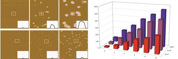
In our research, we have developed a novel approach to produce well defined and functional DNA-heme enzyme conjugates.3,4 To this end, covalent DNA-hemin adducts were synthesized, which were subsequently used to reconstitute apo-myoglobin and horseradish peroxidase. The reconstitution produced highly active enzymes that contained one or two DNA oligomers coupled to the enzyme in close proximity to the active sites. Such DNA-enzyme conjugates were attached to a solid support using the DDI method and the peroxidase activity of the conjugates was investigated. The programmable binding properties enabled by DNA hybridization make such semisynthetic enzyme conjugates useful for a broad range of applications, ranging from biocatalysis, to the development of electrochemical sensors and novel biomaterials.
2. C.M. Niemeyer, Trends Biotechnol. 2002, 20, 295-401.
3. L. Fruk, C.M. Niemeyer, Angew. Chem. Int. Ed. 2005, 44, 2603-2606
4. L. Fruk, J. Müller, C. M. Niemeyer, Chemistry � A European Journal 2006, In Press
One of the grand challenges in nanotechnology is the development of fabrication technologies that will lead to cost effective nanomanufacturing processes. In addition to the more classical top-down processes such as photolithography, so-called bottom-up processes are also being developed for carrying out self-assembly of nanostructures into higher order structures, materials and devices. To this end, considerable efforts have been carried out on Layer-by-Layer (LBL) self-assembly processes as a way to make three dimensional structures which can have macroscopic x-y dimensions. However, limitations of both passive and active LBL self-assembly processes provide considerable incentive to continue the development of better paradigms for nanofabrication and heterogeneous integration. Over the past decade electronic microarray devices, produced by a top-down photolithography process, have been developed for DNA diagnostic applications. In these applications, the electronic microarray device is first used to address and bind negatively charged DNA molecules to selected test-sites on the microarray surface. Target DNA sequences are then rapidly transported and selectively hybridized to the DNA sequences bound at the specific test-sites. Thus, these devices are able to direct and accelerate the self-assembly or 'bottom-up' process of DNA hybridization occurring on the microarray. Electronic microarrays have been used to carry out the transport, addressing and selective binding of a variety of charged biomolecules such as DNA, RNA, biotin/streptavidin, and antibodies; as well as quantum dots, metallic and polymeric nanoparticles; cells and even 20 micron sized light emitting diode (LED) semiconductor devices. Overall, these devices have proven ability to manipulate a surprising large variety of entities that range in size from small molecules to micron scale objects. Now using an advanced 400 site CMOS microarray device and controller system we have demonstrated the rapid and highly parallel assisted self-assembly of DNA and protein derivatized nanoparticles into multi-layer structures. Electronic array based assisted self-assembly represents an example of combining some of the best aspects of 'top-down' and 'bottom-up' technologies into viable process for the hierarchical assembly and integration of nanocomponents into 3D structures. Such a nanofabrication process will be useful for a variety of nanoelectronic, nanophotonic, energy conversion (fuel cells, photovoltaics, batteries), smart/morphing nanocomposite material and in-vivo therapeutic/drug delivery applications. 
2. D. Klinov, B. Dwir, E. Kapon, N. Borovok, T. Molotsky, A. Kotlyar, submitted to Langmuir (2006).
3. A. Kotlyar, N. Borovok, T. Molotsky, D. Klinov, B. Dwir, E. Kapon, Nucleic Acid Res. 33, 6515 (2005).
2. A.Kotlyar, N.Borovok, T.Molotsky, D.Klinov, B.Dwir, E.Kapon, Nucleic Acid Res. 33, 6515 (2005).
b Center for Nano Bioengineering and R&D Center for Membrane Technology, Chung Yuan Christian University, Taiwan, R.O.C.
c National Nanotechnology Lab of INFM, Lecce, Italy
2. Manna L, MillironN DJ, Meisel A, Scher EC, Alivisatos AAP. Controlled growth of tetrapod-branched inorganic nanocrystals. Nature Materials 2003;2(june 2003):382-385.
3. Pellegrino T, Manna L, Kudera S, Liedl T, Koktysh D, Rogach AL, et al. Hydrophobic nanocrystals coated with an amphiphilic polymer shell: a general route to water soluble nanocrystals. Nanoletters 2004;4(4):703-707.
4. Pellegrino T, Kudera S, Liedl T, Javier AM, Manna L, Parak WJ. On the Development of Colloidal Nanoparticles towards Multifunctional Structures and their Possible Use for Biological Applications. Small 2005;1(1):48-63.
b Center for Nano Bioengineering and R&D Center for Membrane Technology, Department of Biomedical Engineering, Chung Yuan Christian University, Taiwan, R.O.C.
c National Nanotechnology Lab of INFM, Lecce, Italy
2 Department of Molecular Science and Engineering, National Taipei University of Technology, Taiwan, ROC
3 Institute of Physics, Academia Sinica, Nankang 11529, Taipei, Taiwan, ROC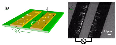
* Regulation et Dynamique des genomes. UMR5153 CNRS-MNHN Paris;
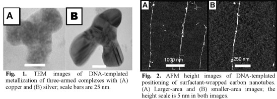
Here we report our recent investigations towards fabrication of SWNT-based circuits templated onto DNA. We will present the set of tools developed to specifically target and bind SWNTs to DNA, using bio-directed non-covalent chemistry through biotin-streptavidin molecular recognition properties. Complementary characterizations by gel electrophoresis, AFM and TEM imaging demonstrate the efficiency of the binding methods. These latter allowed us, for example, to bridge two SWNTs by a DNA molecule or to specifically address a SWNT on a desired location onto DNA. Then, we applied these techniques to precisely address a SWNT on a �m-scale three-armed DNA scaffold, essential starting point for the assembly of simple electronic devices into a circuit context. 
[2] Avouris, Ph. Review article in MRS Bulletin 2004, 29, 403-410.
[3] Keren K., Berman R.S., Buchstab E., Sivan U., Braun E. Science 2003, 21, 1380-1382. Hazani M., Hennrich F., Kappes M., Naaman R., Peled D., Sidorov V., Shvarts D. Chem.Phys.Lett. 2004, 391, 389-392 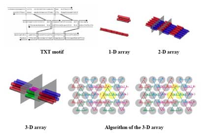
[2] L. Fruk, J. Müller, C.M. Niemeyer, Chemistry, 2006, 12, in press
[2] N. C. Seeman, Nanotechnology 2 (1991), 149-159
[3] C. A. Mirkin, Inorg. Chem. 39 (2000), 2258-2272
[4] J. Richter, M. Mertig, W.Pompe, I. Mönch, H.K. Schackert, App. Phys. Lett. 78 (2001), 536
Analysis of oligonucleotides cleaved from conventional solid supports confirmed that the ferrocenyl-nucleoside remained intact and the resulting strands exhibited reversible electrochemical behaviour. The redox potential of fully solvated ferrocenyl 12-mers, 350 mV versus SCE, was shifted by +40 mV to a more positive potential upon treatment with the complement contrary to the anticipated negative shift based on a simple electrostatic basis.
Automated solid-phase methods were also used to integrate 12-mer ferrocenyl-containing oligonucleotides with silicon <111> electrodes through bifunctional molecular interconnects. Hybridisation to the surface-bound ferrocenyl-DNA again caused a positive shift in the reduction potential of +34 mV, indicating that, even when a ferrocenyl nucleoside is contained in a film, the increased density of anions from the phosphate backbone of the complement is once again dominated by other factors, such as the hydrophobic environment of the ferrocene moiety within the duplex or changes in the ferrocene-phosphate distances. The reduction potential is shifted >100 mV after hybridisation when the aqueous system was replaced by THF/LiClO4, a solvent of much lower dielectric constant; this is consistent with an explanation based on conformation-induced changes in ferrocene�phosphate distances. 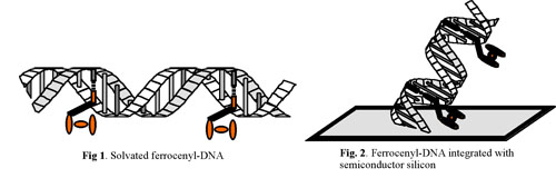
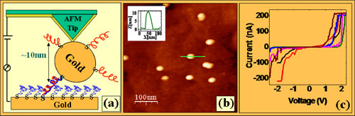
We have developed a method to attach short (26 bp) DNA molecules to a gold surface at one end and to a gold nanoparticle on the other end. Upon approaching and contacting the gold particle with a conductive AFM tip with a controlled applied force, we can measure current-voltage curves through the double-stranded DNA molecule. Our measurements show relatively high currents (200 nA@2 V). We report a comprehensive set of control experiments that support these results. Further we compare the electrical conductivity of monolayers of: ssDNA, dsDNA and dsDNA with thiols in the upper end. The results call for faster conduction mechanism than those suggested to account for the solution chemistry experiments.
One of the attractive DNA derivatives for nanoelectronics is G4-DNA, a molecules composed of consecutive guanine tetrads. I will present clear polarizability measurements in this molecule. If time allows I will also report STM spectroscopy of single DNA molecules.
Here we present a different approach to create defined nano-structures. The process of in-vitro rolling circle amplification via phi29 DNA polymerase offers the possibility to create long sequences of repeating units of single-stranded DNA. To avoid the problem of stretching a long single-stranded DNA-molecule after its synthesis, the amplification-reaction will be carried out under the influence of an external force, starting at a surface-bound primer. The applied external force might for example be an alternating electric field or a hydrodynamic force.
By this approach it should be possible to determine the direction of the synthesis. The product will be fixed at its end at a catching-line of an oligonucleotide-sequence which is complementary to a section in the amplified circular template. Using dip-pen-technology this experiment can be transferred from the micro- to the nano-scale.
[2] Scipioni, A., Pisano, S., Bergia, A., Savino M., Samori, B., and De Santis, P. Sequence-dependent DNA recognition by an inorganic crystal surface in the nanoscale (in pubbl.)
[3] Mao, C., W. Sun, and N.C. Seeman, Designed Two-Dimensional DNA Holliday Junction Arrays Visualized by Atomic Force Microscopy. J. Am. Chem. Soc., 1999. 121: p. 5437-544'.
With this background, applications of SPM for nanomanipulation as well as new developments in SPM instrumentation, specifically designed by Veeco Instruments for advanced biological research, are discussed in this contribution.
Veeco's recently introduced Bioscope TM II SPM is fully compatible with high-end commercial inverted microscope systems, and allows integration of SPM with optical techniques like brightfield, phase contrast, DIC microscopy, and fluorescence techniques, such as confocal and TIRF. The large X-Y scan size of 150 x 150 μm and the 15 μm Z-range in a three-axis closed-loop scanner design permits access to larger biological structures, such as cells. For experiments requiring more stringent control of environmental conditions, a 'soft-seal' perfusion chamber and sample heater facilitates control of both temperature and fluid/gaseous conditions.
Hardware and software of the Bioscope TM II SPM offer high flexibility for imaging and correlation with well known optical techniques, for interaction studies ('point and shoot' feature, force volume function, PicoForce TM molecular pulling), and nanomanipulation with the dedicated NanoManTM user interface.
Among the several key points required to perform SWNTs devices network assembled on DNA scaffold, one of them is to control SWNT-DNA binding. An approach for the functionalization of biological compounds onto the nanotube ends consists in a realization of a covalent coupling via the carboxylic group coming from the oxidative purification.
According to the literature, the amount of defects produced by acidic purification is around 5 % [2-4], which implies that a lot of carboxylic groups are present not only at the nanotube ends but also onto the sidewalls. Based on this point, we performed a study onto the nanotube-DNA coupling varying the ratio of coupling reagent versus defects groups and using surfactant to protect side-wall to determine in which conditions DNA binds selectively to nanotube ends. This binding, realized with EDC / NHS as a coupling reagent, 5'-amino-C6-DNA and TX100 as surfactant, was characterized by an AFM statistical study onto more than 200 functionalized nanotubes for each conditions. It enables us to determine the set of parameters to get more than 85 % DNA strands connected to the nanotube ends.
[2] M. A. Hamon, H. Hu, P. Bhowmik, S. Niyogi, B. Zhao, M. E. Itkis, R. C. Haddon, Chem. Phys. Lett. 2001, 347, 8 -12.
[3] D. B. Mawhinney, V. Naumenko, A. Kuznetsova, J. T. Yates, J. Liu, R. E. Smalley, Chem. Phys. Lett. 2000, 324, 213 -216.
[4] A. Hirch, Angew. Chem. Int. Ed. 2002, 4, 1853-1859.
However, lithographically fabricated electrodes have a minimum line width of tens of nanometers. Since carbon nanotubes (CNT) are only few nanometers in diameter, they can be used as electrodes to produce even higher field gradients. We demonstrate DEP of nanoscale molecules using CNT as an electrode and quantitatively verify the better performance of CNT electrodes in trapping of nanoscale dsDNA, compared to the lithographically fabricated nanoelectrodes, by in situ confocal microscopy. In addition, the attachment of thiol-modified dsDNA was studied with two different linkers between the DNA and thiol group, and also the DEP of various size dsDNA, even as short as 27 bp, was demonstrated. The electrical conductivity of the thiol-modified 140 nm long dsDNA molecules attached between gold electrodes was measured and the effect of humidity was investigated. In dry environment it showed insulating behaviour (See Fig. below), but in moist conditions (RH ~ 80%) the significantly lower resistances were observed [1]. This provides clear evidence of humidity effects on conductivity of individual DNA molecules. Our results also suggest that the effect is related to a humidity induced conformational change of the molecular structure and associated with a contribution from a direct electronic transport.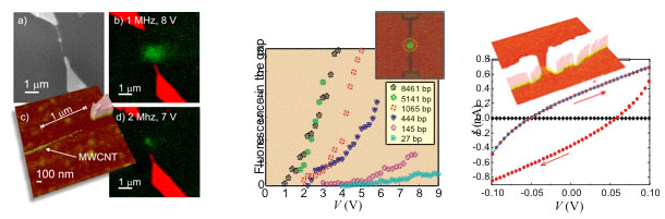
b IPHT-Jena, P.O.B. 100239, 07702 Jena, Germany
Upon appropriate sample preparation the G-wire DNA can make continuous, highly oriented DNA networks. This behavior has not been seen on other types of substrates. One of the challenges of characterizing the conductivity of the G-wire networks is the difficulty of preparing mica substrates with electrical contacts. Microfabrication processes were used to construct two, three, and four point probe epoxy masks with 20 �m gaps. These constructs were used as shadow masks to integrate 15-nm thick sputtered gold contacts into the G-wire DNA networks over the mica surface. Systematic evaluation of G-wire network conductivity is currently underway. 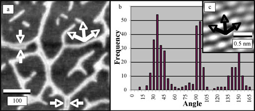
We have studied thiol modified oligonucleotides on Au(111) by single-crystal voltammetry, X-ray photoelectron spectroscopy (XPS), and in situ STM [1-3]. In situ scanning tunnelling microscopy (STM) is an outstanding tool for characterizing the electronic properties of biomolecules in their natural aqueous medium at the single molecule level.
We describe the surface dynamics of a double-strand decanucleotide with ten adenine-thymine base pairs linked to a Au(111)-electrode surface via a hexamethylene thiol linker. The thymine bases of the oligonucleotide are in the locked conformation. Hybridization in solution is effected prior to linking to the Au(111)-surface. The melting point of the linker-free locked decanucleotide is > 63°C. However, all three sets of data suggest that the oligonucleotides dehybridize on binding to the Au(111)-electrode surface. This points to an adsorption mechanism in which a stable high density of Au-S bonds is achieved but at the expense of significant unzipping of the more voluminous duplex form.
[2] H.Wackerbarth, M. Grubb, J. Zhang, A.G. Hansen, and J. Ulstrup Angew. Chem. Int. Ed. 43 (2004) 198.
[3] H.Wackerbarth, M. Grubb. J. Zhang, A.G. Hansen, and J. Ulstrup Langmuir 20 (2004) 1647.
[4] H. Wackerbarth, M. Grubb, J. Wengel, I. Chorkendorff, and J. Ulstrup (2006) Surf. Sci., accepted.